Yao Qiuhong, Lin Liping, Zhao Tingting, Chen Xi. Advances in Preparation, Physicochemical Properties and Applications of Heteroatom-Doped Graphene Quantum Dots[J]. Progress in Chemistry, 2015, 27(11): 1523-1530.
Contents
1 Introduction
2 Preparation methods
2.1 Preparation of single-doped graphene quantum dots
2.2 Preparation of co-doped graphene quantum dots
3 Physicochemical properties of heteroatom-doped graphene quantum dots
3.1 Photoluminescence
3.2 Electrochemiluminescence
3.3 Catalytic property
4 Applications
4.1 Applications in biological field
4.2 Applications in environmental field
4.3 Applications in energy-related field
5 Conclusion and prospect

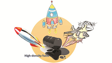
Pan Lun, Deng Qiang, E Xiutianfeng, Nie Genkuo, Zhang Xiangwen, Zou Jijun. Synthesis Chemistry of High-Density Fuels for Aviation and Aerospace Propulsion[J]. Progress in Chemistry, 2015, 27(11): 1531-1541.
Contents
1 Introduction
2 Molecular characteristic of high-density fuels
3 Synthesis of polycyclic hydrocarbon fuels
3.1 Oligomerization reaction
3.2 Hydrogenation reaction
3.3 Isomerization reaction
4 Synthesis of highly strained fuels
4.1 Cyclopropanated hydrocarbons
4.2 Quadricyclane
4.3 Pentacyclo[5.4.0.02,6.03,10.05,9]undecane and dimer
5 Synthesis of high-density biofuels
5.1 Pinene-derived fuels
5.2 Lignocellulose-derived fuels
6 Synthesis of nano-fluid fuels
7 Conclusion
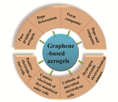
Chen Xiaoyan, Sun Yiran, Yu Fei, Chen Junhong, Ma Jie. The Catalytic Properties for Reduction of Graphene-Based Aerogels and Their Applications[J]. Progress in Chemistry, 2015, 27(11): 1542-1554.
Contents
1 Introduction
2 GA and its catalytic properties
3 Synthesis and modification of catalytical active GA
3.1 Preparation of pure GA
3.2 Preparation of doped GA
3.3 Preparation of GA composite
3.4 Preparation of doped GA composite
4 Applications of GA in reduction catalyst
4.1 Applications in positive electrode of fuel cells
4.2 Applications in counter electrode of dye-sensitized solar cells
4.3 Applications in cathode of microbial electrolysis cells
4.4 Applications in hydrogen peroxide electro-chemical sensors
5 Conclusion and outlook
Zhou Yan, Zhao Xuebing, Liu Dehua. Effects of Non-Ionic Surfactant on the Enzymatic Hydrolysis of Lignocellulose and Corresponding Mechanism[J]. Progress in Chemistry, 2015, 27(11): 1555-1565.
Contents
1 Introduction
2 Effects of surfactant on enzymatic hydrolysis of pure cellulose and mechanism
2.1 Factors influencing the action of surfactant
2.2 Mechanism for the action of surfactant on pure cellulose hydrolysis
3 Effects of surfactant on enzymatic hydrolysis of pretreated lignocellulose
3.1 Effects of substrate structural features
3.2 Effects of hydrolysis conditions
4 Mechanisms for the action of surfactant on lignocellulose hydrolysis
4.1 Effects of surfactant on substrate structure
4.2 Effects of surfactant on enzyme stability
4.3 Effects of surfactant on the interaction between enzyme and substrate
5 Conclusion

Liu Xiaobo, Kou Zongkui, Mu Shichun. Porous Graphene Materials[J]. Progress in Chemistry, 2015, 27(11): 1566-1577.
Contents
1 Introduction
2 Theoretical base and properties of porous graphene
3 Synthesis of porous graphene
3.1 Lithography techniques
3.2 Catalytic etching methods
3.3 Chemical vapor deposition method
3.4 Wet etching
3.5 Carbothermal reduction method
3.6 Solvothermal synthesis
3.7 Free radical attack method
3.8 Other methods
4 Applications
4.1 Fuel cell materials
4.2 Supercapacitors electrode materials
4.3 Lithium ion battery electrode materials
4.4 Field effect transistors
4.5 Chemical sensors
4.6 Water desalination
4.7 Molecular sieve
4.8 DNA sequencing
5 Existing problems
6 Conclusion and perspectives

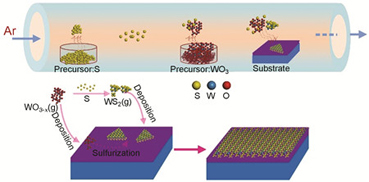
You Yuncheng, Zeng Tian, Liu Jinsong, Hu Tingsong, Tai Guoan. Chemical Vapor Deposition and Application of Graphene-Like Tungsten Disulfide[J]. Progress in Chemistry, 2015, 27(11): 1578-1590.
Contents
1 Introduction
2 Physical Properties of tungsten disulfide thin films
3 Preparation of WS2 thin films via chemical vapor deposition technique
3.1 Classification of chemical vapor deposition technique
3.2 Mechanism of preparing WS2 thin films
4 Application of WS2 thin films in electrical devices
4.1 Field effect transistor
4.2 Photoelectric device
4.3 Heterostructural device
5 Conclusion and outlook
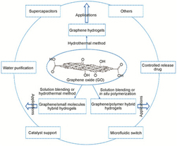
Liu Jingjing, Chu Huijuan, Wei Hongliang, Zhu Hongzheng, Zhu Jing, He Juan. Progress in Graphene-Based Hydrogels[J]. Progress in Chemistry, 2015, 27(11): 1591-1603.
Contents
1 Introduction
2 Categories of graphene-based hydrogels
2.1 Graphene hydrogels
2.2 Graphene/small molecules hybrid hydrogels
2.3 Graphene/macromolecules hybrid hydrogels
3 Applications of graphene-based hydrogels
3.1 Supercapacitor
3.2 Water purification
3.3 Drug-controlled release
3.4 Microfluidic switch
3.5 Catalyst support
3.6 Others
4 Conclusion
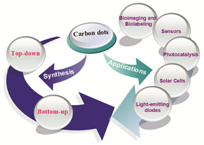
Huang Qitong, Lin Xiaofeng, Li Feiming, Weng Wen, Lin Liping, Hu Shirong. Synthesis and Applications of Carbon Dots[J]. Progress in Chemistry, 2015, 27(11): 1604-1614.
Contents
1 Introduction
2 Synthesis methods of carbon dots
2.1 Top-down methods
2.2 Bottom-up methods
3 Applications of carbon dots
3.1 Bioimaging and Biolabeling
3.2 Sensors
3.3 Photocatalysis
3.4 Solar cells
3.5 Light-emitting diodes
4 Conclusion
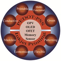
Yang Lei, Cheng Tao, Zeng Wenjin, Lai Wenyong, Huang Wei. Inkjet-Printed Conductive Polymer Films for Optoelectronic Devices[J]. Progress in Chemistry, 2015, 27(11): 1615-1627.
Contents
1 Introduction
2 Inkjet printing of PEDOT:PSS films
2.1 Inkjet printing
2.2 Inkjet-printed PEDOT:PSS films
2.3 Inkjet-printed hybrid electrodes
3 Inkjet-printed PEDOT:PSS films for optoelectronic devices
3.1 Organic field effect transistors(OFET)
3.2 Organic photovoltaics(OPV)
3.3 Organic light-emitting diodes(OLED)
3.4 Organic memory devices
4 Conclusion
Ding Peng, Chen Xian, Li Xiuling, Qing Guangyan, Sun Taolei, Liang Xinmiao. The Separation and Enrichment of Glycoproteins or Glycopeptides Based on Nanoparticles[J]. Progress in Chemistry, 2015, 27(11): 1628-1639.
Contents
1 Introduction
2 The separation and enrichment of glycoproteins or glycopeptides based on nanoparticles
2.1 Detonation nanodiamond(dND)
2.2 Magnetic nanoparticls
2.3 Polymer nanoparticles
2.4 Gold nanoparticles
2.5 SiO2 nanoparticles
2.6 TiO2 nanoparticles
2.7 Glycopeptide enrichment:methods comparison
3 Conclusion and outlook
Yu Jing, Ha Wei, Shi Yanping. Intelligent Hydrogel-Based Dual Drug Delivery System[J]. Progress in Chemistry, 2015, 27(11): 1640-1648.
Contents
1 Introduction
2 Intelligent hydrogel-based dual drug delivery carriers
2.1 Temperature-sensitive carriers
2.2 pH sensitive carriers
2.3 Redox sensitive carriers
3 The means of drug combination in hydrogel
3.1 Combination of two anticancer drugs
3.2 Combination of anticancer drug and growth factor
3.3 Combination of anticancer drug and gene
4 Conclusion

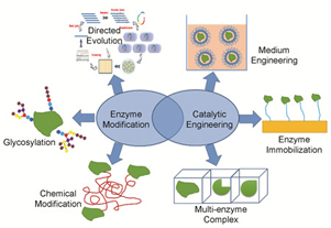
Feng Xudong, Li Chun. The Improvement of Enzyme Properties and Its Catalytic Engineering Strategy[J]. Progress in Chemistry, 2015, 27(11): 1649-1657.
Contents
1 Introduction
2 Current application of enzymes
3 Enzyme modification
3.1 Directed evolution
3.2 Glycosylation
3.3 Chemical modification
4 Catalytic engineering of enzymes
4.1 Medium engineering
4.2 Immobilization
4.3 Multi-enzyme complex
5 Conclusion
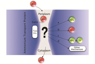
Zhang Mingming, Fan Jianfen, Yu Yi, Yan Xiliang, Xu Jian. Studying on the Mechanisms of NH3/NH4+through Ammonium Transport Proteins[J]. Progress in Chemistry, 2015, 27(11): 1658-1664.
Contents
1 Introduction
2 NH3 transport mechanism
3 NH4+ transport mechanism
4 Cooperative transport of NH3 and H+
5 Other transport mechanisms
6 Conclusion
Liu Yu, Fu Ruiqi, Lou Zimo, Fang Wenzhe, Wang Zhuoxing, Xu Xinhua. Preparation of Functional Carbon-Based Materials for Removal of Heavy Metals from Aqueous Solution[J]. Progress in Chemistry, 2015, 27(11): 1665-1678.
Contents
1 Introduction
2 Preparation of functional carbon-based materials for removal of heavy metals from aqueous solution
2.1 Functional activated carbon
2.2 Functional graphene
2.3 Functional carbon nanotubes
2.4 Functional biochar
3 The influencing factors of heavy metal removal from water by functional carbon-based materials
3.1 The properties of composite materials
3.2 Environmental conditions
4 The application of functional carbon-based materials
5 Conclusion and outlook

Jiang Binbo, Yuan Shiling, Chen Nan, Wang Haibo, Wang Jingdai, Huang Zhengliang. Reaction Kinetics of n-Butane Oxidation on VPO Catalyst[J]. Progress in Chemistry, 2015, 27(11): 1679-1688.
Contents
1 Introduction
2 Catalytic mechanism
3 Reaction network
3.1 Triangle reaction network
3.2 Reaction network involving furan route
3.3 Reaction network involving alkoxide route and furan route
4 Reaction kinetics
4.1 The exploration period
4.2 The forming period
4.3 The further developing period
5 Conclusion


