中文
Announcement
More
Progress in Chemistry 2015, Vol. 27 Issue (11): 1578-1590 DOI: 10.7536/PC150433 Previous Articles   Next Articles

• Review and comments •

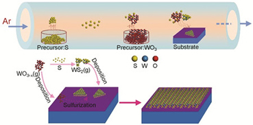
Chemical Vapor Deposition and Application of Graphene-Like Tungsten Disulfide

You Yuncheng1,2, Zeng Tian1,2, Liu Jinsong2, Hu Tingsong2, Tai Guoan1*   

  1. 1. State Key Laboratory of Mechanics and Control of Mechanical Structures, Key Laboratory for Intelligent Nano Materials and Devices of the Ministry of Education and Institute of Nanoscience, Nanjing University of Aeronautics and Astronautics, Nanjing 210016, China;
    2. College of Material Science and Technology, Nanjing University of Aeronautics and Astronautics, Nanjing 210016, China
  • Received: Revised: Online: Published:
  • Supported by:
    The work was supported by the Fundamental Research Funds for the Central Universities(No.NS2013095).
PDF ( 2226 ) Cited
Export

EndNote

Ris

BibTeX

Graphene-like transition metal chalcogenide compounds such as MoS2, WS2, MoSe2, WSe2 have attracted wide interests because of their unique layer number-dependent bandgap. In particularly, intrinsic WS2 is a bipolar semiconductor with n-type and p-type electronic transport properties, it is expected to be widely used in electrical circuit, memory, photodetector and photovoltaic devices. Recently, chemical vapor deposition(CVD) technique, in contrast to traditional chemical or physical exfoliation options, is extensively used to prepare large-area two-dimensional transition metal chalcogenide(such as MoS2, MoSe2, WS2 and WSe2) atomic layers. Although a few review papers about other two-dimensional materials have been published, the detailed introduction for graphene-like WS2 has been rarely reported. In this review, we summarize the research progress on chemical vapor deposition and related devices of graphene-like WS2. First, we introduce two growth methods of preparing WS2 thin films via chemical vapor deposition techniques: two-step growth route and one-step growth route, and then discuss the growth mechanism of the two methods and essential parameters that influence the growth of the WS2 thin films such as sulfur content, carrier gas composition, reaction temperature and substrate materials. Then, we introduce the research progress of WS2-based transistors, photoelectric devices and related heterostructures. Finally, we analyze and review possible problems in developing WS2-related devices.

Contents
1 Introduction
2 Physical Properties of tungsten disulfide thin films
3 Preparation of WS2 thin films via chemical vapor deposition technique
3.1 Classification of chemical vapor deposition technique
3.2 Mechanism of preparing WS2 thin films
4 Application of WS2 thin films in electrical devices
4.1 Field effect transistor
4.2 Photoelectric device
4.3 Heterostructural device
5 Conclusion and outlook

CLC Number: 

[1] Novoselov K S, Geim A K, Morozov S V, Jiang D, Zhang Y, Dubonos S V, Grigorieva I V, Firsov A A. Science, 2004, 306:666.
[2] Zhang Y, Tan Y W, Stormer H L, Kim P. Nature, 2005, 438:201.
[3] Lee C, Wei X, Kysar J W, Hone J. Science, 2008, 321:385.
[4] Novoselov K S, Geim A K, Morozov S V, Jiang D, Katsnelson M I, Grigorieva I V, Dubonos S V, Firsov A A. Nature, 2005, 438:197.
[5] 张芸秋(Zhang Y Q),梁勇明(Liang Y M),周建新(Zhou J X). 化学学报(Acta Chim. Sinica), 2014, 72:357.
[6] Wang Q H, Kalantar-Zadeh K, Kis A, Coleman J N, Strano M S. Nat. Nanotechnol., 2012, 7:699.
[7] Ge W, Kawahara K, Tsuji M, Ago H. Nanoscale, 2013, 5:5773.
[8] 史建平(Shi J P), 马冬林(Ma D L), 张艳锋(Zhang Y F), 刘忠范(Liu Z F). 化学学报(Acta Chim. Sinica), 2015, DOI:10.6023/A15030157.
[9] 王新胜(Wang X S), 谢黎明(Xie L M), 张锦(Zhang J). 化学学报(Acta Chim. Sinica), 2015, DOI:10.6023/A15030187.
[10] Splendiani A, Sun L, Zhang Y, Li T, Kim J, Chim C Y, Galli G, Wang F. Nano Lett., 2010, 10:1271.
[11] Radisavljevic B, Radenovic A, Brivio J, Giacometti V, Kis A. Nat. Nanotechnol., 2011, 6:147.
[12] Novoselov K S, Jiang D, Schedin F, Booth T J, Khotkevich V V, Morozov S V, Geim A K. Proc. Nat. Acad. Sci. U. S. A., 2005, 102:10451.
[13] Eda G, Yamaguchi H, Voiry D, Fujita T, Chen M, Chhowalla M. Nano Lett., 2011, 11:5111.
[14] Zeng Z, Yin Z, Huang X, Li H, He Q, Lu G, Boey F, Zhang H. Angew. Chem. Int. Ed., 2011, 50:11093.
[15] Coleman J N, Lotya M, Neill A O, Bergin S D, King P J, Khan U, Young K, Gaucher A, De S, Smith R J, Shvets I V, Arora S K, Stanton G, Kim H Y, Lee K, Kim G T, Duesberg G S, Hallam T, Boland J J, Wang J J, Donegan J F, J C, Moriarty G, Shmeliov A, Nicholls R J, Perkins J M, Grieveson E M, Theuwissen K, McComb D W, Nellist P D, Nicolosi V. Science, 2011, 331:568.
[16] Hussain A M, Sevilla G A T, Rader K R, Hussain M M. Chemical Vapor Deposition based Tungsten Disulfide(WS2) Thin Film Transistor(Eds. BenSaleh1 M S, Qasim S M), Fira:IEEE, 2013. 1.
[17] Sorkin V, Pan. H, Shi H, Quek S Y, Zhang Y W. Crit. Rev. Solid State Mater. Sci., 2014, 39:319.
[18] Zhao W, Ghorannevis Z, Amara K K, Pang J R, Toh M, Zhang X, Eda G. Nanoscale, 2013, 5:9677.
[19] Shanmugam M, Bansal T, Durcan C A, Yu B. Appl. Phys. Lett., 2012, 101:263902.
[20] Berkdemir A, Gutiérrez H R, Botello-Méndez A R, Perea-López N, Elías A L, Chia C I, Wang B, Crespi V H, López-Urías F, Charlier J C, Terrones H, Terrones M. Sci. Rep., 2013, 3:1755.
[21] Zhao W, Ribeiro R M, Eda G. Acc. Chem. Res., 2015, 48:91.
[22] Kuc A, Zibouche N, Heine T. Phys. Rev. B, 2011, 83:45213.
[23] Ji Q, Zhang Y, Zhang Y, Liu Z. Chem. Soc. Rev., 2015, 44:2587.
[24] Shi Y, Li H, Li L J. Chem. Soc. Rev., 2015, 44:2744.
[25] Cong C, Shang J, Wu X, Cao B, Peimyoo N, Qiu C, Sun L, Yu T. Adv. Opt. Mater., 2014, 2:131.
[26] Okada M, Sawazaki T, Watanabe K, Taniguch T, Hibino H, Shinohara H, Kitaura R. ACS Nano, 2014, 8:8273.
[27] Shanmugam M, Jacobs-Gedrim R, Song E S, Yu B. Nanoscale, 2014, 6:12682.
[28] Shanmugam M, Bansal T, Durcan C A, Yu B. Appl. Phys. Lett., 2012, 101:263902.
[29] Orofeo C M, Suzuki S, Sekine Y, Hibino H. Appl. Phys. Lett., 2014, 105:083112.
[30] Elías A L, Perea-López N, Castro-Beltrán A, Berkdemir A, Lv R, Feng S, Long A D, Sayashi T, Kim Y A, Endo M, Gutiérrez H R, Pradhan N R, Balicas L, Mallouk T E, López-Urías F, Terrones H, Terrones M. ACS Nano, 2013, 7:5235.
[31] Gutiérrez H R, Perea-López N, Elías A L, Berkdemir A,Wang B, Lv R, López-Urías F, Crespi V H, Terrones H, Terrones, M. Nano Lett., 2013, 13:3447.
[32] Song J G, Park J, Lee W, Choi T, Jung H, Lee C W, Hwang S H, Myoung J M, Jung J H, Kim J H, Lansalot-Matras C, Kim H. ACS Nano, 2013, 7:11333.
[33] Rong Y, Fan Y, Koh A L, Robertson A W, He K,Wang S, Tan H, Sinclair R, Warner J H. Nanoscale, 2014, 6:12096.
[34] Jung Y, Shen J, Liu Y, Woods J M, Sun Y, Cha J J. Nano Lett., 2014, 14:6842.
[35] Zhang Y, Zhang Y, Ji Q, Ju J, Yuan H, Shi J, Gao T, Ma D, Liu M, Chen Y, Song X, Hwang H Y, Cui Y, Liu Z. ACS Nano, 2013, 7:8963.
[36] Vander Vlies A J, Kishan G, Niemantsverdriet J W, Prins R, Weber T. J. Phys. Chem. B, 2002, 106:3449.
[37] Ovchinnikov D, Allain A, Huang Y S, Dumcenco D, Kis A. ACS Nano, 2014, 8:8174.
[38] Liu X, Hu J, Yue C, Della Fera N, Ling Y, Mao Z, Wei J. ACS Nano, 2014, 8:10396.
[39] Braga D, Gutiérrez Lezama I, Berger H, Morpurgo A. F. Nano Lett., 2012, 12:5218.
[40] 唐晶晶(Tang J J), 第凤(Di F), 徐潇(Xu X), 肖迎红(Xiao Y H), 车剑飞(Che J F). 化学进展(Progress in Chemistry), 2012, 24:501.
[41] Koppens F H L, Mueller T, Avouris P, Ferrari A C, Vitiello M S, Polini M. Nat. Nanotechnol., 2014, 9:780.
[42] Sang Y, Zhao Z, Zhao M, Hao P, Leng Y, Liu H. Adv. Mater., 2015, 27:363.
[43] Lee S H, Lee D, Hwang W S, Hwang E, Jena D, Yoo W J. Appl. Phys. Lett., 2014, 104:193113.
[44] Britnell L, Ribeiro R M, Eckmann A, Jalil R, Belle B D, Mishchenko A, Kim Y-J, Gorbachev R V, Georgiou T, Morozov S V, Grigorenko A N, Geim A K, Casiraghi C, Castro Neto A H, Novoselov K S. Science, 2013, 340:1311.
[45] Perea-López N, Elías A L, Berkdemir A, Castro-Beltran A, Gutiérrez H R, Feng S, Lv R, Hayashi T, López-Urías F, Ghosh S, Muchharla B, Talapatra S, Terrones H, Terrones M. Adv. Funct. Mater., 2013, 23:5511.
[46] Yin Z Y, Li H, Li H, Jiang L, Shi Y M, Sun Y H, Lu G, Zhang Q, Chen X D, Zhang H. ACS Nano, 2012, 6:74.
[47] Cao B, Shen X, Shang J, Cong C, Yang W, Eginligil M, Yu T. APL Mater., 2014, 2:116101.
[48] Geim A K, Grigorieva I V. Nature, 2013, 499:419.
[49] Georgiou T, Jalil R, Belle B D, Britnell L, Gorbachev R V, Morozov S V, Kim Y J, Gholinia A, Haigh S J, Makarovsky O, Eaves L, Ponomarenko L A, Geim A K, Novoselov K S, Mishchenko A. Nat. Nanotechnol., 2013, 8:100.
[50] Duan X, Wang C, Shaw J C, Cheng R, Chen Y, Li H, Wu X, Tang Y, Zhang Q, Pan A, Jiang J, Yu R, Huang Y, Duan X. Nat. Nanotechnol., 2014, 9:1024.
[51] Hong X, Kim J, Shi S F, Zhang Y, Jin C, Sun Y, Tongay S, Wu J, Zhang Y, Wang F. Nat. Nanotechnol., 2014, 9:682.
[52] Yuan J, Najmaei S, Zhang Z, Zhang J, Lei S M, Ajayan P, Yakobson B I, Lou J. ACS Nano, 2015, 9:555.
[53] Tongay S, Fan W, Kang J, Park J, Koldemir U, Suh J, Narang D S, Liu K, Ji J, Li J, Sinclair R, Wu J. Nano Lett., 2014, 14:3185.
[54] Jung Y, Shen J, Sun Y, Cha J J. ACS Nano, 2014, 8:9550.
[1] Hui Zhang, Shanshan Wang, Jinshan Yu. Low-Symmetry Two-Dimensional ReS2 and its Heterostructures:Chemical Vapor Deposition Synthesis and Properties [J]. Progress in Chemistry, 2022, 34(6): 1440-1452.
[2] Xiujun Cao, Lei Zhang, Yuanxin Zhu, Xin Zhang, Chaonan Lv, Changmin Hou. Design and Synthesis of Sillenite-Based Micro/Nanomaterials and Their Applications in Photocatalysis [J]. Progress in Chemistry, 2020, 32(2/3): 262-273.
[3] Qi Zhang, Huiqing Xiang, Jianguo Liu, Xiaoyan Zeng. Materials System for Inkjet Printing High Performance Thin-Film Transistors [J]. Progress in Chemistry, 2019, 31(10): 1417-1424.
[4] Qingyang Xi, Jinsong Liu, Ziquan Li, Kongjun Zhu, Guoan Tai, Ruogu Song. Etching Methods and Application of Molybdenum Disulfide Film [J]. Progress in Chemistry, 2018, 30(6): 847-863.
[5] Yufu Chen, Xianggao Li, Yin Xiao, Shirong Wang. Solution Processed Large-Scale Small Molecular Organic Field-Effect Transistors [J]. Progress in Chemistry, 2017, 29(4): 359-372.
[6] Gaobo Lin, Ting Luo, Lvbing Yuan, Wenjie Liang*, Hai Xu*. High Performance n-Type and Ambipolar Small Organic Semiconductors for Organic Field-Effect Transistors [J]. Progress in Chemistry, 2017, 29(11): 1316-1330.
[7] Wenjie Zhu, Guoan Tai, Xufeng Wang, Qilin Gu, Zenghui Wu, Kongjun Zhu. Fabrication and Strain Sensing Properties of Two-Dimensional Atomic Crystal Materials [J]. Progress in Chemistry, 2017, 29(11): 1285-1296.
[8] Zeng Tian, You Yuncheng, Wang Xufeng, Hu Tingsong, Tai Guoan. Chemical Vapor Deposition and Device Application of Two-Dimensional Molybdenum Disulfide-Based Atomic Crystals [J]. Progress in Chemistry, 2016, 28(4): 459-470.
[9] Yang Lei, Cheng Tao, Zeng Wenjin, Lai Wenyong, Huang Wei. Inkjet-Printed Conductive Polymer Films for Optoelectronic Devices [J]. Progress in Chemistry, 2015, 27(11): 1615-1627.
[10] Song Jingyi, Jiang Lang*, Dong Huanli, Hu Wenping*. Organic Micro- and Nano-Crystal Field-Effect Transistors [J]. Progress in Chemistry, 2013, 25(01): 12-27.
[11] Yang Liu, Lei Ting, Pei Jian*, Liu Chenjiang* . Design Strategy , Processing and Applications of Organic Micro- and Nano-Materials [J]. Progress in Chemistry, 2012, 24(12): 2299-2311.
[12] Cai Xiaozhou, Jiang Lang, Dong Huanli, Li Jingze*, Hu Wenping* . Organic Circuits and Their Basic Elements [J]. Progress in Chemistry, 2012, 24(12): 2431-2442.
[13] Feng Yan, Wu Qingsong, Zhang Guoying, Sun yaqiu. Visible-Light Responsed Bi2WO6 Photocatalysts [J]. Progress in Chemistry, 2012, 24(11): 2124-2131.
[14] Liu Jie Jiang Lang Hu Wenping. The Application of Anthracene and Its Derivatives in Organic Field-Effect Transistors [J]. Progress in Chemistry, 2009, 21(12): 2568-2577.
[15] Li Rongjin1, Li Hongxiang1,Zhou Xinran2,Hu Wenping 1*. Polymer Field-Effect Transistors:Materials and Devices [J]. Progress in Chemistry, 2007, 19(0203): 325-336.