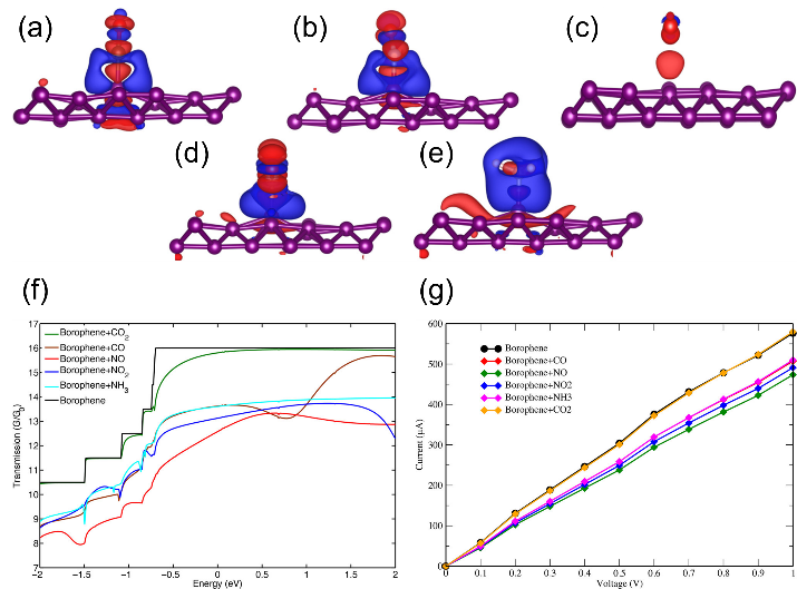
| 2D Materials | Structural characteristics | Physical characteristics | Potential application | ref |
|---|---|---|---|---|
| Borophene | Structural diversity More stable after hydrogenation | Dirac cones Larger Young’s modulus Superconductivity | Energy storage Nanoscale gas sensor Biomedical applications | |
| Silicene | Low buckled geometry | Dirac cones High Fermi velocity and carrier mobility Spin-orbit coupling Ambipolar Dirac charge transport | Field effect transistor Spintronic devices | |
| Germanene | Low buckled geometry | Resistance to atmospheric oxidation | Energy storage and catalysis | |
| Phosphorene | Vertically skewed/wrinkled honeycomb structure | Semiconductor with a predicted direct bandgap Layer dependent photoluminescence Superior mechanical flexibility | Phosphorene-based devices | |
| Hexagonal boron nitride | Hexagonal structure | Electrical insulation Excellent thermal conductivity | Substrates and gate dielectrics for 2D electronics applications Super-capacitor | |
| Transition metal dihalides | Containing triangular and honeycomb transition metal nets | High temperature paramagnetic behavior | Kitaev spin liquid |
Fig. 1 Schematic diagram and physical characterization of γ-B28 borophene: (a) Schematic diagram of preparation and structure of γ-B28 borophene; (b) AFM images; (c) FFT images; (d) Ultraviolet-visible (UV-Vis) absorption spectrum; (e) Room temperature photoluminescence (PL) spectrum[
Fig. 3 Crystal structure of borophene on mica substrates: (a) Atomic structure diagram of borophene and mica; (b) Structure of α′-2H borophene; (c) AFM image of borophene; (d) HRTEM image of borophene; (e) TEM image of borophene. Corresponding SAED images are shown as insets[
Fig. 4 Typical TEM images of few-layer B nanosheets prepared by 4 h tip ultrasonication in DMF (a, b) and IPA (c, d), followed by centrifugation at 5000 r/min for 30 min. The insets in (a), (c), and (d) display the corresponding FFT patterns of the selected regions[
Fig. 5 Synthesis of αʹ-4H-borophene by in-situ thermal decomposition: (a) SEM image; (b) Statistical data of lateral dimensions of 80 nanosheets measured by SEM; (c) AFM image; (d) Low-resolution TEM image; (e) HRTEM image and corresponding SAED pattern; (f) Reconstructed HRTEM image of the FFT pattern extracted from the red rectangular region in (e)[
Fig. 6 Morphology and crystallinity of borophene-graphene heterostructures: (a~c) SEM images of few-layer graphene, borophene, and borophene-graphene heterostructure; (d) Low-resolution TEM image of a typical borophene-graphene heterostructure; (e) Low-resolution TEM image of borophene; (f) HRTEM image extracted from the green rectangular region in (e). Insets show the corresponding SAED patterns and HRTEM images obtained from computational models; (g~i) STEM-HAADF-EDS elemental mapping of the borophene-graphene heterostructure[
Fig. 7 (a~e) Charge density difference maps of gas adsorption (CO, NO, CO2, NO2, NH3) on the surface of borophene. Red surfaces indicate electron gain, while blue surfaces indicate electron loss; (f) Zero-bias transmission of pristine borophene and borophene+gas system; (g) I-V characteristics of monolayer borophene with different adsorbed gas molecules[
Fig. 10 Borophene-graphene heterostructure humidity sensor: (a) Schematic representation of the sensor based on borophene-graphene heterostructure; (b) Humidity sensing behavior of the heterostructure sensor at different relative humidities; (c) Sensitivity of the heterostructure sensor exposed to different relative humidities; (d) Response and recovery curves of the heterostructure sensor under 85% RH; (e) Schematic diagram of the bent heterostructure sensor on a PET substrate; (f) Response curves of the sensor with and without applied bending strain[
Fig. 11 Borophene-BC2N heterostructure humidity sensor: (a) Real-time response of the sensor at different humidity levels; (b) Long-term response of the sensor at different humidity levels; (c) Real-time current curve of the sensor as the fingertip approaches at different distances[