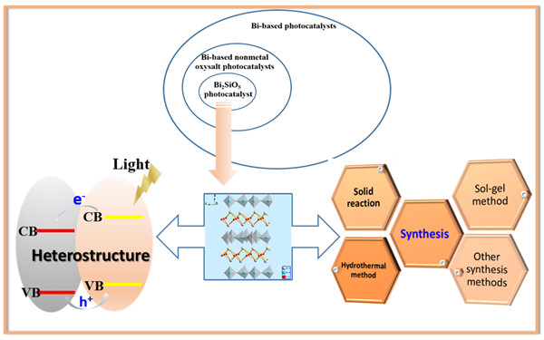
Di Liu, Qian Liu, Yonggang Wang, Yongfa Zhu. Bi2SiO5 Semiconductor Photocatalyst[J]. Progress in Chemistry, 2018, 30(6): 703-709.
Fanfan Du, Ying Zheng, Guorong Shan, Yongzhong Bao, Suyun Jie*, Pengju Pan*. Hydrogen Bonding-Based Non-Metallic Organocatalysts for Ring-Opening Polymerization of Lactones[J]. Progress in Chemistry, 2018, 30(6): 710-718.

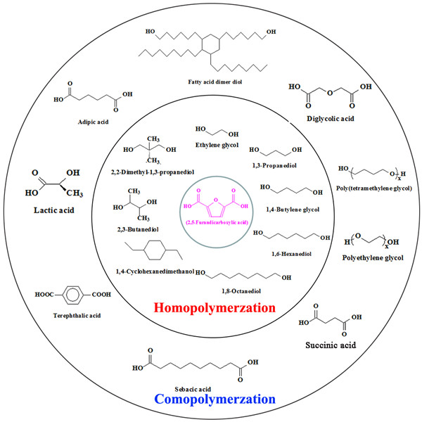
Guoqiang Wang, Min Jiang*, Qiang Zhang, Rui Wang, Xiaoling Qu, Guangyuan Zhou*. Polyesters Containing Furan Rings Based on Renewable Resources[J]. Progress in Chemistry, 2018, 30(6): 719-736.
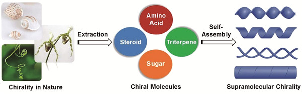
Yuxia Gao, Yun Liang, Jun Hu, Yong Ju. Supramolecular Chiral Self-Assembly Based on Small Molecular Natural Products[J]. Progress in Chemistry, 2018, 30(6): 737-752.
Ting Wang, Rui Xue, Yuli Wei, Mingyue Wang, Hao Guo, Wu Yang. Development and Applications of Covalent Organic Frameworks(COFs) Materials: Gas Storage, Catalysis and Chemical Sensing[J]. Progress in Chemistry, 2018, 30(6): 753-764.
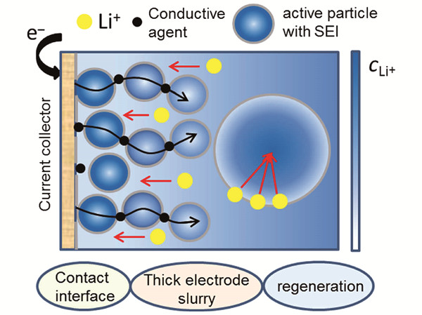
Dandan Liu, Yongchong Chen, Han He, Yingyuan He, Hao Liu, Bin Zhang. Scientific Fundamentals of Lithium Slurry Battery[J]. Progress in Chemistry, 2018, 30(6): 765-774.
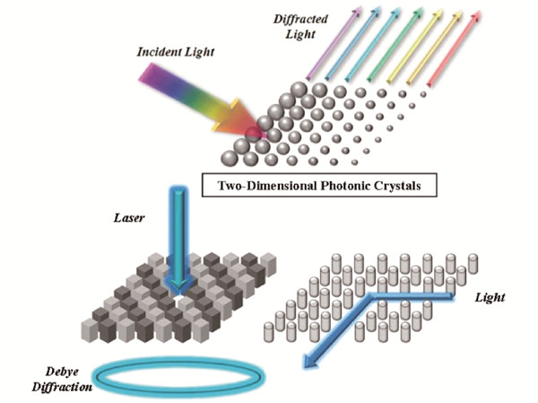
Cheng Chen, Zhiqiang Dong, Haowen Chen, Yang Chen, Zhigang Zhu, Weiheng Shih. Two-Dimensional Photonic Crystals[J]. Progress in Chemistry, 2018, 30(6): 775-784.
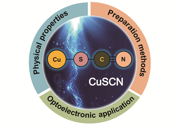
Yuanyuan Qi, Mingguang Li, Honglei Wang, Wen Zhang, Runfeng Chen*, Wei Huang*. Applications of Novel Hole-Transporting Material Copper(Ⅰ) Thiocyanate (CuSCN) in Optoelectronic Devices[J]. Progress in Chemistry, 2018, 30(6): 785-796.
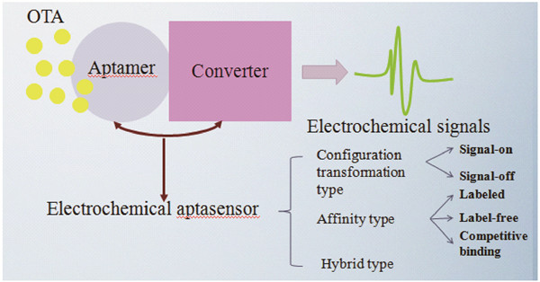
Yanqun Shan, Xiaoying Wang*. Electrochemical Aptasensor for Detection of Ochratoxin A[J]. Progress in Chemistry, 2018, 30(6): 797-808.
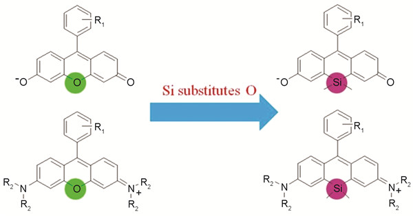
Man Du, Baolong Huo, Jiemin Liu*, Mengwen Li, Leqiu Fang, Yunxu Yang*. Fluorescent Probes Based on Silicon-Substituted Xanthene Dyes and Their Applications in Bioimaging[J]. Progress in Chemistry, 2018, 30(6): 809-830.
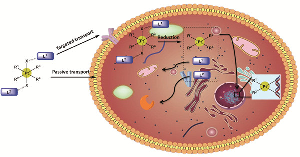
Xiaoxiao Tan, Guoshuai Li, Qingpeng Wang, Bingquan Wang, Dacheng Li, Peng George Wang. Small Molecular Platinum(Ⅳ) Compounds as Antitumor Agents[J]. Progress in Chemistry, 2018, 30(6): 831-846.
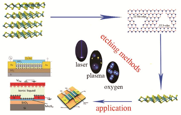
Qingyang Xi, Jinsong Liu, Ziquan Li, Kongjun Zhu, Guoan Tai, Ruogu Song. Etching Methods and Application of Molybdenum Disulfide Film[J]. Progress in Chemistry, 2018, 30(6): 847-863.
Xiao Li, Ling Ai, Jing Zhang, Xianpeng Zhang, Yuehui Lu, Weijie Song. Transparent Antifogging Materials[J]. Progress in Chemistry, 2018, 30(6): 864-871.
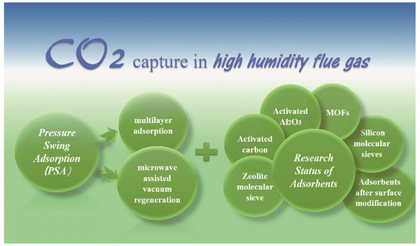
Liying Liu, He Gong, Zhe Wang, Gang Li, Tao Du. Application of Pressure Swing Adsorption Technology to Capture CO2 in Highly Humid Flue Gas[J]. Progress in Chemistry, 2018, 30(6): 872-878.