


1 引言
2 红外光探测器件类型与工作原理
2.1 有机光电晶体管
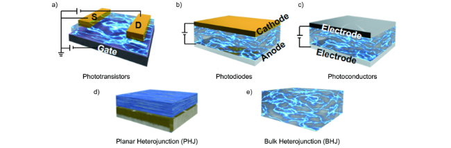
2.2 有机光电二极管
2.3 有机光导
3 红外光探测器的性能参数
表1 红外光探测器关键参数的总结Table 1 Summary of key parameters in infrared detector |
| parameter | formula |
|---|---|
| responsivity(R) | R=Iph/Pin |
| external quantum efficiency(EQE) | EQE=Iphhc/Pinλq = Rhc/λq |
| sensitivity(P) | P=Iph/Idark |
| noise equivalent power(NEP) | NEP=Iin/R |
| specific detectivity(D*) | D*=(S1/2R)/(2e ) D*=R(Sƒ)1/2/ |
| rise time(τr) | — |
| decay time(τd) | — |
| linear dynamic range(LDR) | LDR = 20log(Iph,max/Iph,min) LDR = log2(Iph,max/Iph,min) LDR = 10log(Pin,max/NEP) |
| photoconductive gain(G) | G = τr/τt |
| cut-off frequency(f-3db) | — |
4 面向红外光的有机复合材料
4.1 有机光电晶体管的活性层材料
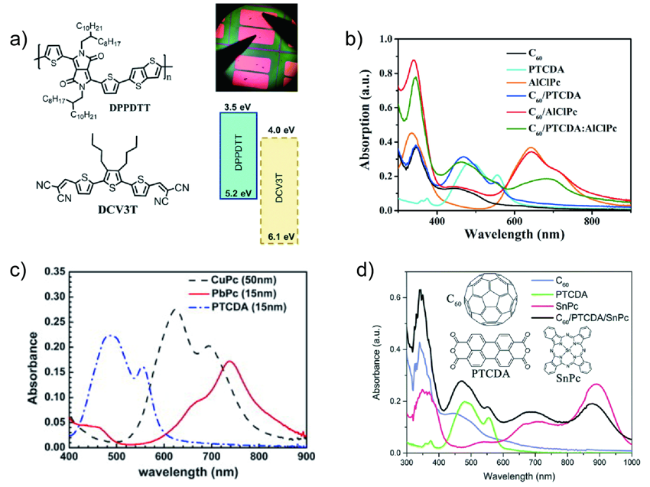
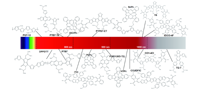
图2 a) 所测器件的光学照片,DPPDTT和DCV3T的能级排列和分子结构[12];b~d) 器件中活性层的UV-vis-NIR光谱[31⇓~33]Fig. 2 a) Optical image of testing device, molecular structure, and energy level of DPPDTT, and DCV3T[12].Copyright 2021, Royal Society of Chemistry. b) The UV-Vis-NIR absorption spectra of active layers of the device[31⇓~33]. Copyright 2018, Royal Society of Chemistry. Copyright 2013, Elsevier. Copyright 2017, Elsevier |
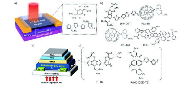
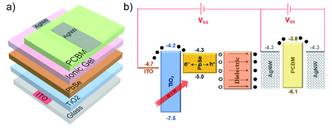
图3 a) 基于PQT-12/F4-TCNQ活性层的红外光电晶体管的结构示意图[34];b) PC61BM, DPP-DTT, PC71BM, ITIC and PCBM的分子结构图[37] [38],;c) 全聚合物光电晶体管的结构示意图,d)PTB7、P(NDI2OD-T2)的分子结构图[39]Fig. 3 a) Schematic diagram of organic IR phototransistor based on PQT-12/F4-TCNQ[34]; b) molecular structure of PC61BM, DPP-DTT, PC71BM, ITIC and PCBM[37] [38], c) Schematic diagram of all-polymer phototransistor, d) chemical structures of PTB7 and P(NDI2OD-T2)[39]. Copyright 2021, John Wiley and Sons. Copyright 2013, Royal Society of Chemistry. Copyright 2022, Elsevier. Copyright 2017, American Chemical Society. |
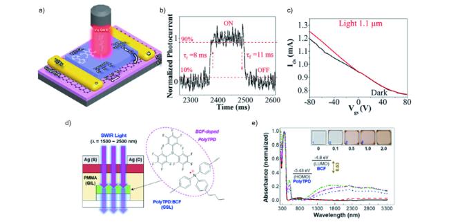
图4 a,b) TTF-CA/graphene 混合光电晶体管示意图和光响应时间测试;c) 在暗态和光照下的IDS vs VG 曲线[40];d) 器件的结构示意图以及PolyTPD和 BCF的分子结构示意图;e) 具有不同BCF比例的PolyTPD:BCF薄膜涂覆于石英基底的光学照片[41]Fig. 4 a,b) Illustration and photoresponse time measurement of a TTF-CA/graphene hybrid phototransistor; c) IDS vs VG curves in the dark and under light[40]; d) Schematic of device structure and the molecular structure of PolyTPD and BCF; e) photographs of PolyTPD:BCF films coated on quartz substrates with different BCF molar ratio[41]. Copyright 2020, John Wiley and Sons. Copyright 2021, Royal Society of Chemistry. |
4.2 有机光电二极管的活性层材料
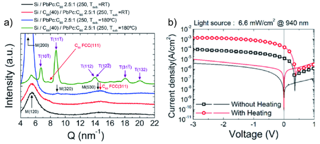
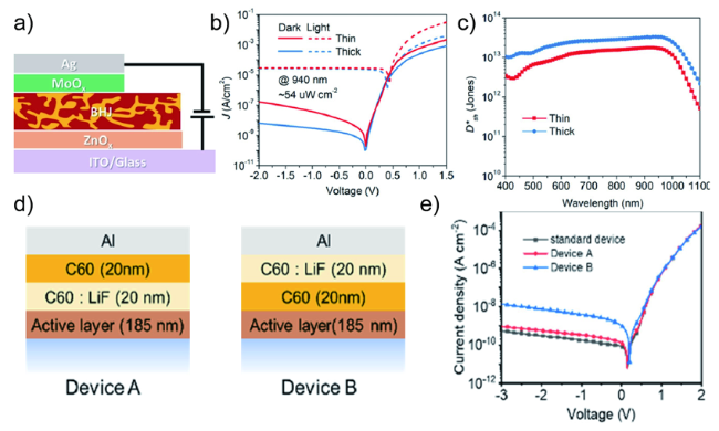
图8 a) 基于PTB7-Th:CO1-4Cl光电二极管的结构示意图;b) 在暗态及光照下的电流密度和电压曲线;c)在-0.1 V测得的短噪音限制的比探测度[51]; d,e) 不同活性层器件的示意图以及相对应的J-V曲线[52]Fig. 8 a) Device structure of OPDs based on PTB7-Th:CO1-4Cl. b) J-V curves of the OPDs in the dark and under illumination of NIR. c) Shot-noise-limited specific detectivity of the OPDs at -0.1 V[51]. d,e) Schemes and respective J-V curves of devices with different active layers[52]. Copyright 2020, John Wiley and Sons. Copyright 2021, American Chemical Society |
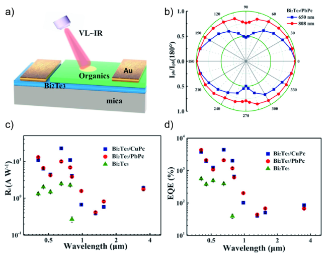
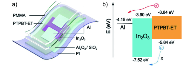
图9 a) 3维拓扑绝缘体/有机薄膜异质结光探测器的结构示意图;b) Bi2Te3/有机薄膜异质结器件的线性偏振表征;c,d) 在偏压模式下Bi2Te3/PbPc、Bi2Te3/CuPc、和Bi2Te3 的Ri、EQE曲线[57]Fig. 9 a) Structure diagram of 3D topological insulators/organics thin film heterojunction photodetectors. b) Linear polarization characteristics of the Bi2Te3/organics thin film heterojunction devices. c,d) Ri, EQE curves of Bi2Te3/PbPc, Bi2Te3/CuPc, and Bi2Te3 photodetectors under Vbias mode[57]. Copyright 2019, American Chemical Society |
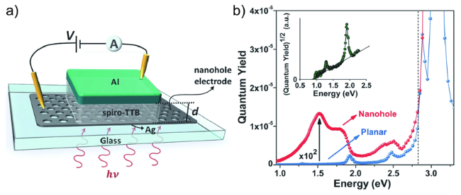
图10 a) 有机层spiro-TTB在一个有纳米孔Ag电极和一个反射Al电极中间夹层的三明治结构的器件示意图;b) 具有纳米孔电极器件和平面电极器件的EQE图谱,插图是量子效率的平方根随光子能量的函数图[22]Fig. 10 a) Structure diagram of an organic (spiro-TTB) layer sandwiched between a nanohole Ag electrode and a reflective Al electrode. b) EQE spectra of the nanohole device and of the planar device. The inset is the square root of the quantum yield as a function of photon energy[22].Copyright 2016, John Wiley and Sons |
5 红外光电器件的应用
5.1 人工视网膜
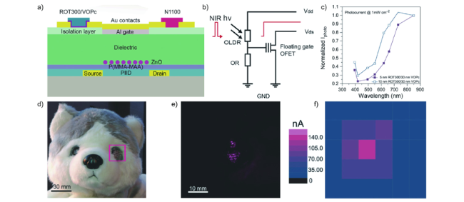
图12 a) 有机视网膜类的光传感器示意图以及其活性层组成;b) 光传感器的电路示意图;c) ROT300/VOPc光探测器的随入射波长变化的归一化后的光电流图;d)哈士奇毛绒玩具瞳孔上覆有转移人工视网膜;e) 有一束光照射到哈士奇瞳孔后的图片;f) 用有30个像素的源漏电流测试哈士奇玩偶瞳孔的近红外强度分布[63]Fig. 12 a) Schematic of the organic, retina-like photosensor with the active layers’ composition. b) Electric diagram of photosensor. c) Normalized photocurrent versus incident wavelength of ROT300/VOPc photodetector. d) The pupil of a husky stuffed toy with transferred artificial retina. e) The husky pupil with a light pulse shedding on. f) The NIR intensity distribution over the husky toy pupil measured by drain-source currents with 30 pixels[63]. Copyright 2017, John Wiley and Sons |
5.2 人工突触
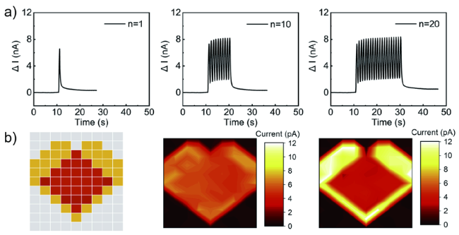
图13 a)通过增加脉冲光激发的次数诱导出的短期记忆到长期记忆的转变;b)加密图案示意图;c)在915 nm 刺激 1 次及在1342 nm刺激5次;d)同时在915 nm和1342 nm刺激5 次[64]Fig. 13 a) The STM (short-term memory)-to-LTM (long-term memory) transition induced by increasing the number of pulsed light stimuli. b) Schematic illustration of image pattern. c) Input image encoded by 915 nm stimulus 1 time and 1342 nm stimulus 5 times. d) Input image encoded by both 915 nm stimulus and 1342 nm stimulus 5 times, respectively.[64] Copyright 2017, Elsevier |
5.3 光电逻辑电路
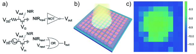
图14 a)基于光电晶体管的逻辑电路:“非”门(上)和“或”门(下);b)光电晶体管阵列示意图,可以用于呈现从一个LED灯泡发出的光分布;c)在LED照射下光电晶体管的光电流图[43]Fig. 14 a) Circuit diagrams based on the phototransistor. NOT gate (top) and OR gate (bottom). b) Schematic illustration of phototransistor array which is for imaging the light distribution from a LED lamp. c) The photocurrent mapping of the phototransistor array under the LED illumination[43]. Copyright 2021, John Wiley and Sons |
5.4 光电容积脉搏波
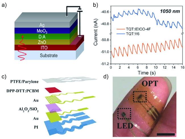
图15 a)柔性有机光电晶体管的器件结构示意图;b)在手指表皮外包覆hPPG传感器的光学照片(比例尺,5 mm)[66];c) 具有反型结构的BHJ器件结构示意图;在有环境光并且休息状态下,用1050 nm LEDs测得的PPG图[54]Fig. 15 a) Schematic of the device structure of the flexible OPT. b) Photograph of a finger covered with the epidermal hPPG (hybrid organic/inorganic NIR photoplethysmogram) sensor (scale bar, 5 mm)[66]. c) Schematic of the BHJ device structure with inverted architecture. d) PPG (Photoplethysmograms) taken under normal (resting) conditions and ambient light using 1050 nm LEDs and OPDs[54]. Copyright 2017, John Wiley and Sons. Copyright 2022, John Wiley and Sons. |