中文
Announcement
More
Progress in Chemistry 2024, Vol. 36 Issue (2): 204-223 DOI: 10.7536/PC230616 Previous Articles   Next Articles

• 24 •

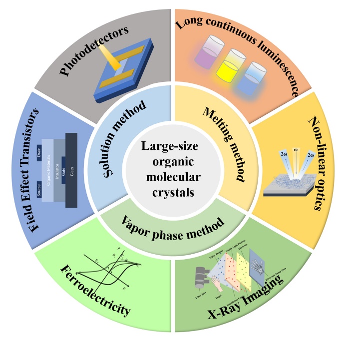
Growth of Large-Size Organic Molecular Crystals for Optoelectronic Applications

Jingyu Cui1, Hui Jiang2, Rongjin Li1, Weigang Zhu1()   

  1. 1 Key Laboratory of Organic Integrated Circuits, Ministry of Education, Tianjin Key Laboratory of Molecular Optoelectronic Sciences, Department of Chemistry, School of Science, Tianjin University, Tianjin 300072, China
    2 School of Materials Science and Engineering, Tianjin University, Tianjin 300072, China
  • Received: Revised: Online: Published:
  • Contact: *e-mail: w_zhu10@tju.edu.cn
  • Supported by:
    National Natural Science Foundation of China(U21A6002)
Richhtml ( 3 ) PDF ( 61 ) Cited
Export

EndNote

Ris

BibTeX

Organic molecular crystals, bounded together by non-covalent interactions, are three-dimensional long-range ordering and thermodynamic stable, and have low defect density and show rich prospects for applications in organic field effect transistors (OFETs), X-ray imaging, nonlinear optics, optical waveguides, flexible wearable devices, and lasers. However, previous research is mainly based on organic bulk crystals or small-size crystals, and there is less research on large-size organic molecular crystals while practical application scenarios often require large-size organic molecular crystals, such as transistor arrays and circuits requiring inch-level crystal films, X-ray imaging and nonlinear optical frequency conversion require centimeter-level crystals. However, it is difficult to obtain high-quality large-size organic molecular crystals, and there is no summary and review on the growth and optoelectronic properties of large-size organic molecular crystals at home and abroad. In this review, we first introduce the growth mechanism and growth method of molecular crystals, followed by the materials for growing large-size organic molecular crystals. Then we summarize the applications of large-size organic molecular crystals in optoelectronic aspects, such as long-persistent luminescence, nonlinear optics, X-ray imaging, fast neutron detection, field-effect transistors, and photodetectors. Finally, the challenges in this field are discussed and an outlook on future development is provided.

Contents

1 Introduction

2 Growth mechanism and method

2.1 Theory of crystal growth

2.2 Growth methods

3 Classical organic molecular materials

3.1 Materials for Bulk single crystals

3.2 Materials for single crystal films

4 Optoelectronic applications

4.1 Long-Persistent Luminescence

4.2 Non-linear optical response

4.3 X-Ray Imaging

4.4 Fast neutron detection

4.5 Ferroelectricity

4.6 Field-Effect Transistors and Circuits

4.7 Photodetectors

5 Conclusion and outlook

Fig. 1 Development trend of optoelectronic functional crystal materials: From inorganic crystals to organic crystals, from micro and nano crystals to large size crystals
Fig.2 Optical microscope images of the nonclassical crystallization in the: a) nucleation, b~d) fusion, and e) growth stage. f, g) Polarizing microscope images of a concave-shaped crystal in the fusion stage. h, i) The corresponding AFM images. j) A schematic of a typical concentration-temperature curve. k) Supersaturation ratio as a function of time, by which a step-change of S was introduced by the two-step procedure[30]. Copyright ? 2022 The Authors. Advanced Electronic Materials published by Wiley‐VCH GmbH
Table 1 Summary of Crystal Growth Techniques
Fig. 3 Principle of Crystal Growth by Bridgman Method (a) Basic structure; (b) Temperature distribution. Tm is the melting point of the crystal.
Fig. 4 Cut and polished single crystal of benzimidazole[33]. Copyright ? 2004 Elsevier B.V. All rights reserved.
Fig. 5 Sketches of the SCS method for the growth and transfer of 2DMC. (a) A floating lens was formed when a droplet of solution was placed on the surface of DI water. (b) Enhanced spreading with surfactant in the DI water. (c) 2D crystallization resulted in the growth of 2DMC. (d) Transfer of the 2DMC to the target substrate[38]. Copyright ? 2018, American Chemical Society
Fig. 6 Four main steps of crystal growth by vapor phase meth
Fig. 7 Scheme of the physical vapor transport growth method. (a) Open system. The material is heated in zone 1 and sublimed in a flow of carrier gas under pressures ranging from a few Torr (few hPa) to atmospheric pressure. The molecular vapor crystallizes downstream at a lower temperature in zone 2, with pure crystals separated from impurities due to the temperature gradient and the flow of the carrier gas. (b) Closed system. The material (impurities and the compound of interest) is heated in a sealed glass/quartz ampoule. (c) Semi-closed system. The materials are sealed in a glass ampoule, but a small orifice in the ampoule allows impurities and a portion of the crystallizing material to escape from the ampoule. Zone 1: Sublimation zone; zone 2: Crystal growth zone[48]. Copyright ? 2013, The Materials Research Society
Fig. 8 Pentacene-doped p-terphenyl crystals[52]. Copyright ? 2020, American Chemical Society
Fig. 9 Optical images of a) CuPc, b) F4CuPc, c) F8CuPc, d) F16CuPc single crystals[54]. Copyright ? 2017 WILEY‐VCH Verlag GmbH & Co. KGaA, Weinheim
Fig. 10 (a) Urea doped (10 mol%) L-cysteine hydrochlorid- emonohydrate single crystal[55] Copyright ? 2015 Elsevier B.V. All rights reserved. (b) Photograph of OHB-T crystal[56]. Copyright ? 2020 Elsevier B.V. All rights reserved.
Fig. 11 The main materials mentioned in this paper for growing large-size organic molecular crystals
Fig. 12 a) Schematic process of carrier transport at the electrode/Cn-DNTT interface. b) Inch-sized 1L-crystals deposited on a SiO2 wafer. c~f) CPOM images of 1L-crystals of Cn-DNTTs, n = 6, 8,10, and 12, respectively. White crossed arrows denote the position of the polarizer and analyzer[58]. Copyright ? 2022 Wiley‐VCH GmbH
Fig. 13 a) Diagram of drop-casting onto water surface. b) Optical microscope image of a ZCC cocrystal film. c), d) Polarized optical microscope images of the ZCC cocrystal film. e) AFM image of a typical ZCC film. f) TEM and its corresponding SAED images of a ZCC film[64]. Copyright ? 2020 Wiley‐VCH GmbH
Fig. 14 The main materials mentioned in this paper for growing large-area organic molecular crystal films
Fig. 15 Schematic diagram of the principle of X-ray imaging in medical diagnosis
Fig. 16 Practical application of the organic semiconductor single crystals for X-ray imaging. a) X-ray images of linear mask taken by 9,10-DPA crystals. b) Light-intensity function of pixels (along the red line above and FWHM is taken as the resolution) patterned millimeter-scale mask. c, d) X-ray images taken by 9,10-DPA single-crystal-based X-ray detector for the university logo. e) System schematic excited by an X-ray synchrotron radiation source. f) X-ray imaging for the circuit board; the red numbers indicate the corresponding position photos and X-ray imaging. g) X-ray imaging for dried small shrimp. h) SEM image of dried small shrimp. i) Calcium mapping and j) oxygen mapping of the shrimp tail[71]. Copyright ? 2021 Wiley‐VCH GmbH
Fig. 17 Representative pulses (a) and pulse-height spectra (b) under Cs-137 and Cf-252 irradiation. The inset of (b) is a partial enlargement for TPE[74]. Copyright ? 2022 Elsevier Inc.
Fig. 18 Transistor characteristics of the 2DCOS. Typical transfer and output characteristics of the OFETs based on the 2DCOS, a), b) perylene, c), d) C6-DPA, e), f) C6-PTA, g), h) C6-DBTDT on OTS SAM modified Si/SiO2 substrates. The different colored lines in (a) (c) (e), and (g) correspond to the different gate voltages[81]. Copyright ? 2016 WILEY‐VCH Verlag GmbH & Co. KGaA, Weinheim
Fig. 19 (a) Photograph of a bulk single crystal of (TMHD)BiBr5. (b) Diagram of planar-type single-crystal photodetector device based on highly oriented (TMHD)BiBr5 single crystal[83]. Copyright ? 2018 WILEY‐VCH Verlag GmbH & Co. KGaA, Weinheim
[1]
Cheng Y, Zhang X, Qin Y X, Dong P, Yao W, Matz J, Ajayan P M, Shen J F, Ye M X. Nat. Commun., 2021, 12: 4092.

doi: 10.1038/s41467-021-24388-y
[2]
Jiang T, Wang Y R, Zheng Y S, Wang L, He X, Li L Q, Deng Y F, Dong H L, Tian H K, Geng Y H, Xie L H, Lei Y, Ling H F, Ji D Y, Hu W P. Nat. Commun., 2023, 14: 2281.

doi: 10.1038/s41467-023-37973-0
[3]
Xu X Z, Deng W, Zhang X J, Huang L M, Wang W, Jia R F, Wu D, Zhang X H, Jie J S, Lee S T. ACS Nano, 2019, 13(5): 5910.

doi: 10.1021/acsnano.9b01734
[4]
Farah S, Doloff J C, Müller P, Sadraei A, Han H J, Olafson K, Vyas K, Tam H H, Hollister-Lock J, Kowalski P S, Griffin M, Meng A, McAvoy M, Graham A C, McGarrigle J, Oberholzer J, Weir G C, Greiner D L, Langer R, Anderson D G. Nat. Mater., 2019, 18(8): 892.

doi: 10.1038/s41563-019-0377-5
[5]
Im H, Yoon J, Choi J, Kim J, Baek S, Park D H, Park W, Kim S. Adv. Mater., 2021, 33 (44): e2102542.
[6]
Marinkas P L. Nature, 1966, 211(5055): 1288.

doi: 10.1038/2111288a0
[7]
Lv B L, Liu Z Y, Tian H, Xu Y, Wu D, Sun Y H. Adv. Funct. Mater., 2010, 20(22): 3987.

doi: 10.1002/adfm.v20.22
[8]
Li Z H, Zeng J H, Li Y D. Small, 2007, 3(3): 438.

doi: 10.1002/smll.v3:3
[9]
Oh C G, Baek Y, Ihm S K. Adv. Mater., 2005, 17(3): 270.

doi: 10.1002/adma.v17:3
[10]
Watanabe T, Cho W S, Suchanek W L, Endo M, Ikuma Y, Yoshimura M. Solid State Sci., 2001, 3(1/2): 183.

doi: 10.1016/S1293-2558(00)01126-2
[11]
Bouaita R, Alombert-Goget G, Ghezal E A, Nehari A, Benamara O, Benchiheub M, Cagnoli G, Yamamoto K, Xu X, Motto-Ros V, Li H, Dujardin C, Lebbou K. CrystEngComm, 2019, 21(28): 4200.

doi: 10.1039/C9CE00510B
[12]
Feigelson R S. J. Cryst. Growth, 2022, 594: 126800.

doi: 10.1016/j.jcrysgro.2022.126800
[13]
Zhu W G, Zhu L Y, Zou Y, Wu Y S, Zhen Y G, Dong H L, Fu H B, Wei Z X, Shi Q, Hu W P. Adv. Mater., 2016, 28(28): 5954.

doi: 10.1002/adma.v28.28
[14]
Cui S Y. Doctoral Dissertation of Shandong University, 2021.
(崔双月. 山东大学博士论文, 2021.)
[15]
Dou Z F, Masteral Dissertation of University of Electronic Science and Technology of China, 2022.
(窦子凡. 电子科技大学硕士论文, 2022.)
[16]
De Yoreo J. A Perspective on Multistep Pathways of Nucleation. In Crystallization via Nonclassical Pathways. Nucleation, Assembly, Observation & Application, American Chemical Society, 2020, 1.
[17]
Tsarfati Y, Biran I, Wiedenbeck E, Houben L, Cölfen H, Rybtchinski B. ACS Cent. Sci., 2021, 7(5): 900.

doi: 10.1021/acscentsci.1c00254
[18]
Ma T Q, Wei L, Liang L, Yin S, Xu L, Niu J, Xue H D, Wang X G, Sun J L, Zhang Y B, Wang W. Nat. Commun., 2020, 11: 6128.

doi: 10.1038/s41467-020-19858-8
[19]
Xue D F, Su L B, Xu J. J. Inorg. Mater., 2023, 38(3): 225.
[20]
Wang W H. Prog. Phys., 2013, 33(5): 177.
汪卫华. 物理学进展, 2013, 33(5): 177.)
[21]
Zhao J P. Design and preparation technology of new functional materials. Beijing: Chemical Industry Press, 2003.
(赵九蓬. 新型功能材料设计与制备工艺. 北京: 化学工业出版社, 2003.)
[22]
Jie W Q. Principle and Technology of Crystal Growth. 2nd ed. Beijing: Science Press, 2019.
(介万奇. 晶体生长原理与技术. 2版. 北京: 科学出版社, 2019.)
[23]
Donnay J D H, Harker D. Am Mineral, 1937, 22 (5): 446.
[24]
Hartman P G. P W, On the relations between structure and morphology of crystal II. 1955.
[25]
Parker R. Crystal Growth: An Introduction. P. Hartman North-Holland, Amsterdam, 1973, 531.
[26]
Hartman P, Bennema P. J. Cryst. Growth, 1980, 49(1): 145.

doi: 10.1016/0022-0248(80)90075-5
[27]
Tocher F E. Mineral. Mag., 1978, 42(321): 165.
[28]
Zheng Y Q, Shi E W, Li W J, Wang B G, Hu X F. Journal of Inorganic Materials, 1999, 03: 321.
(郑燕青, 施尔畏, 李汶军, 王步国, 胡行方. 无机材料学报, 1999, 03: 321.)
[29]
Shi E W, Zhong W Z, Hua S K, Yuan R L, Wang B G, Xia C T, Li W J. Chinese Science, 1998, 01: 37.
施尔畏, 仲维卓, 华素坤, 元如林, 王步国, 夏长泰, 李汶军. 中国科学, 1998, 01: 37.)
[30]
Yao J R, Tian X Z, Li B, Wang Z F, Zhang X L, Jie J S, Yang F X, Li R J, Hu W P. Adv. Electron. Mater., 2023, 9(2): 2201027.
[31]
Scriven L E, Sternling C V. Nature, 1960, 187(4733): 186.

doi: 10.1038/187186a0
[32]
Fan F Q, Zhang Z H, Guo J, Zhang L Y, Zhang X M, Wang T Q, Fu Y. CrystEngComm, 2023, 25(19): 2877.

doi: 10.1039/D3CE00166K
[33]
Vijayan N, Balamurugan N, Ramesh Babu R, Gopalakrishnan R, Ramasamy P, Harrison W T A. J. Cryst. Growth, 2004, 267(1/2): 218.

doi: 10.1016/j.jcrysgro.2004.03.064
[34]
Cui S Y, Zhu T W, Zhang L L, Ye X, Han Q X, Ge C, Guo Q, Zheng X X, Lin Q L, Li C C, Jiang J K, Yuan W Z, Liu Y, Tao X T. Adv. Opt. Mater., 2022, 10(9): 2102355.
[35]
Senthil K, Kalainathan S, Ruban Kumar A. J. Therm. Anal. Calorim., 2014, 118(1): 323.
[36]
Halliwell C A, Dann S E, Ferrando-Soria J, Plasser F, Yendall K, Ramos-Fernandez E V, Vladisavljević G T, Elsegood M R J, Fernandez A. Angew. Chem. Int. Ed., 2022, 61(47): 2208677.
[37]
Mohammed A V, Arulappan J A P, Ganesan S T. Optik, 2015, 126(23): 4322.

doi: 10.1016/j.ijleo.2015.08.026
[38]
Wang Q Q, Yang F X, Zhang Y, Chen M X, Zhang X T, Lei S B, Li R J, Hu W P. J. Am. Chem. Soc., 2018, 140(16): 5339.

doi: 10.1021/jacs.8b01997
[39]
Yao J, Zhang Y, Tian X, Zhang X, Zhao H, Zhang X, Jie J, Wang X, Li R, Hu W. Angew. Chem. Int. Ed., 2019, 58 (45): 16082.

doi: 10.1002/anie.v58.45
[40]
Sele C W, Charlotte Kjellander B K, Niesen B, Thornton M J, van der Putten J B P H, Myny K, Wondergem H J, Moser A, Resel R, van Breemen A J J M, van Aerle N, Heremans P, Anthony J E, Gelinck G H. Adv. Mater., 2009, 21(48): 4926.

doi: 10.1002/adma.v21:48
[41]
Marszalek T, Nosal A, Pfattner R, Jung J, Kotarba S, Mas-Torrent M, Krause B, Veciana J, Gazicki-Lipman M, Crickert C, Schmidt G, Rovira C, Ulanski J. Org. Electron., 2012, 13(1): 121.

doi: 10.1016/j.orgel.2011.10.001
[42]
Qi Z, Zhang F J, Di C A, Wang J Z, Zhu D B. J. Mater. Chem. C, 2013, 1(18): 3072.

doi: 10.1039/c3tc30357h
[43]
Khim D, Han H, Baeg K J, Kim J, Kwak S W, Kim D Y, Noh Y Y. Adv. Mater., 2013, 25(31): 4302.

doi: 10.1002/adma.v25.31
[44]
Hong S, Yi M J, Kang H, Kong J, Lee W, Kim J R, Lee K. Sol. Energy Mater. Sol. Cells, 2014, 126: 107.

doi: 10.1016/j.solmat.2014.03.042
[45]
Lee W Y, Oh J H, Suraru S L, Chen W C, Würthner F, Bao Z N. Adv. Funct. Mater., 2011, 21(21): 4173.

doi: 10.1002/adfm.v21.21
[46]
Kang B, Min H, Seo U, Lee J, Park N, Cho K, Lee H S. Adv. Mater., 2013, 25(30): 4117.

doi: 10.1002/adma.v25.30
[47]
Park Y, Park J, Cho S, Sung M M. Appl. Surf. Sci., 2019, 494: 1023.

doi: 10.1016/j.apsusc.2019.07.184
[48]
Jiang H, Kloc C. MRS Bull., 2013, 38(1): 28.

doi: 10.1557/mrs.2012.308
[49]
Karl N. J. Cryst. Growth, 1990, 99(1/4): 1009.

doi: 10.1016/S0022-0248(08)80072-3
[50]
Laudise R A, Kloc C, Simpkins P G, Siegrist T. J. Cryst. Growth, 1998, 187(3/4): 449.

doi: 10.1016/S0022-0248(98)00034-7
[51]
Wang H, Xie Z Q, Yang B, Shen F Z, Li Y P, Ma Y G. CrystEngComm, 2008, 10(9): 1252.

doi: 10.1039/b805512b
[52]
Cui S Y, Liu Y, Li G L, Han Q X, Ge C, Zhang L L, Guo Q, Ye X, Tao X T. Cryst. Growth Des., 2020, 20(2): 783.

doi: 10.1021/acs.cgd.9b01190
[53]
Deng W, Lei H, Zhang X, Sheng F, Shi J, Zhang X, Liu X, Grigorian S, Zhang X, Jie J S. Adv. Mater., 2022, 34 (13): e2109818.
[54]
Jiang H, Hu P, Ye J, Li Y, Li H, Zhang X, Li R, Dong H, Hu W, Kloc C. Adv. Mater., 2017, 29 (10): 1605053.
[55]
Verma S, Ramachandra Rao K, Kar S, Bartwal K S. Spectrochim. Acta Part A Mol. Biomol. Spectrosc., 2016, 153: 16.

doi: 10.1016/j.saa.2015.08.003
[56]
Xu K, Cao L F, You F, Zhong D G, Wang T H, Yu Z, Hu C, Tang J, Teng B. J. Cryst. Growth, 2020, 547: 125757.

doi: 10.1016/j.jcrysgro.2020.125757
[57]
Kim G, Kim D, Choi Y, Ghorai A, Park G, Jeong U. Adv. Mater., 2023, 35 (4): e2203373.
[58]
Peng B Y, He Z F, Chen M, Chan P K L. Adv. Funct. Mater., 2022, 32(39): 2202632.
[59]
Saha S, Desiraju G R. J. Am. Chem. Soc., 2018, 140(20): 6361.

doi: 10.1021/jacs.8b02435
[60]
Wang Y, Zhu W G, Du W N, Liu X F, Zhang X T, Dong H L, Hu W P. Angew. Chem. Int. Ed., 2018, 57(15): 3963.

doi: 10.1002/anie.v57.15
[61]
Yang F X, Sun L J, Duan Q X, Dong H L, Jing Z K, Yang Y C, Li R J, Zhang X T, Hu W P, Chua L. SmartMat, 2021, 2(1): 99.

doi: 10.1002/smm2.v2.1
[62]
Zhu W G, Zhu L Y, Sun L J, Zhen Y G, Dong H L, Wei Z X, Hu W P. Angew. Chem. Int. Ed., 2016, 55(45): 14023.

doi: 10.1002/anie.v55.45
[63]
Zhu W G, Zheng R H, Zhen Y G, Yu Z Y, Dong H L, Fu H B, Shi Q, Hu W P. J. Am. Chem. Soc., 2015, 137(34): 11038.

doi: 10.1021/jacs.5b05586
[64]
Wang Y, Wu H, Zhu W G, Zhang X T, Liu Z Y, Wu Y S, Feng C F, Dang Y F, Dong H L, Fu H B, Hu W P. Angew. Chem. Int. Ed., 2021, 60(12): 6344.

doi: 10.1002/anie.v60.12
[65]
Bolton O, Lee K, Kim H J, Lin K Y, Kim J. Nat. Chem., 2011, 3(3): 205.

doi: 10.1038/nchem.984
[66]
Wang H, Hu R X, Pang X, Gao H Y, Jin W J. CrystEngComm, 2014, 16(34): 7942.

doi: 10.1039/C4CE00813H
[67]
Cunningham P D, Hayden L M. Opt. Express, 2010, 18(23): 23620.

doi: 10.1364/OE.18.023620
[68]
Wang W L, Wang M, Huang W D. Opt. Mater., 2004, 27(3): 609.

doi: 10.1016/j.optmat.2004.08.072
[69]
Lee S H, Lee S J, Jazbinsek M, Kang B J, Rotermund F, Kwon O P. CrystEngComm, 2016, 18(38): 7311.

doi: 10.1039/C6CE00958A
[70]
Wang J X, Bakr O M, Mohammed O F. Matter, 2022, 5(8): 2547.

doi: 10.1016/j.matt.2022.06.062
[71]
Chen M, Sun L, Ou X, Yang H, Liu X, Dong H, Hu W, Duan X. Adv. Mater., 2021, 33 (43): e2104749.
[72]
Liu Y C, Xu Z, Yang Z, Zhang Y X, Cui J, He Y H, Ye H C, Zhao K, Sun H M, Lu R, Liu M, Kanatzidis M G, Liu S Z. Matter, 2020, 3(1): 180.

doi: 10.1016/j.matt.2020.04.017
[73]
Zhao D, Cai P K, Cheng W, Jia W B, Zhang B B, Zhu M H, Liu L Y, Ouyang X, Sellin P, Jie W Q, Xu Y D. Adv. Funct. Mater., 2022, 32(7): 2108857.
[74]
Sun Q S, Hao Z R, Li J, Liu Z Y, Wang H W, Zhang X T, Li L Q, Dong H L, Hu W P. Matter, 2023, 6(1): 274.

doi: 10.1016/j.matt.2022.10.010
[75]
Wang Z X, Liao W Q. Science, 2022, 375(6587): 1353.

doi: 10.1126/science.abn7440
[76]
Tressler J F, Alkoy S, Newnham R E. J. Electroceram., 1998, 2(4): 257.

doi: 10.1023/A:1009926623551
[77]
Lv H P, Liao W Q, You Y M, Xiong R G. J. Am. Chem. Soc., 2022, 144(48): 22325.

doi: 10.1021/jacs.2c11213
[78]
Tayi A S, Shveyd A K, Sue A C H, Szarko J M, Rolczynski B S, Cao D, Kennedy T J, Sarjeant A A, Stern C L, Paxton W F, Wu W, Dey S K, Fahrenbach A C, Guest J R, Mohseni H, Chen L X, Wang K L, Stoddart J F, Stupp S I. Nature, 2012, 488(7412): 485.

doi: 10.1038/nature11395
[79]
Briseno A L, Mannsfeld S C B, Ling M M, Liu S H, Tseng R J, Reese C, Roberts M E, Yang Y, Wudl F, Bao Z N. Nature, 2006, 444(7121): 913.

doi: 10.1038/nature05427
[80]
Du C, Li L Q, Wang W C, Zhang J D, Yan D H, Hu W P, Fuchs H, Chi L F. AIP Adv., 2012, 2(2): 022138.

doi: 10.1063/1.4723851
[81]
Xu C H, He P, Liu J, Cui A J, Dong H L, Zhen Y G, Chen W, Hu W P. Angew. Chem. Int. Ed., 2016, 55(33): 9443.

doi: 10.1002/anie.v55.33
[82]
Yamamura A, Watanabe S, Uno M, Mitani M, Mitsui C, Tsurumi J, Isahaya N, Kanaoka Y, Okamoto T, Takeya J. Sci. Adv., 2018, 4(2): eaao5758.
[83]
Ji C, Wang P, Wu Z, Sun Z, Li L, Zhang J, Hu W, Hong M, Luo J. Adv. Funct. Mater., 2018, 28(14): 1705467.

doi: 10.1002/adfm.v28.14
[84]
Chen Y Z, Wang S W, Su T Y, Lee S H, Chen C W, Yang C H, Wang K Y, Kuo H C, Chueh Y L. Small, 2018, 14(22): 1704052.
[85]
Chen Y Z, You Y T, Chen P J, Li D P, Su T Y, Lee L, Shih Y C, Chen C W, Chang C C, Wang Y C, Hong C Y, Wei T C, Ho J C, Wei K H, Shen C H, Chueh Y L. ACS Appl. Mater. Interfaces, 2018, 10(41): 35477.

doi: 10.1021/acsami.8b11676
[86]
Ouyang W, Teng F, Fang X. Adv. Funct. Mater., 2018, 28 (16): 1707178.
[87]
Yang W, Chen J, Zhang Y, Zhang Y, He J H, Fang X. Adv. Funct. Mater., 2019, 29 (18): 1808182.

doi: 10.1002/adfm.v29.18
[88]
Oxborrow M, Breeze J D, Alford N M. Nature, 2012, 488(7411): 353.

doi: 10.1038/nature11339
[1] Qingyang Xi, Jinsong Liu, Ziquan Li, Kongjun Zhu, Guoan Tai, Ruogu Song. Etching Methods and Application of Molybdenum Disulfide Film [J]. Progress in Chemistry, 2018, 30(6): 847-863.
[2] Yang Lei, Cheng Tao, Zeng Wenjin, Lai Wenyong, Huang Wei. Inkjet-Printed Conductive Polymer Films for Optoelectronic Devices [J]. Progress in Chemistry, 2015, 27(11): 1615-1627.
[3] Zhu Weigang, Zhen Yonggang, Dong Huanli, Fu Hongbing, Hu Wenping. Organic Cocrystal Optoelectronic Materials and Devices [J]. Progress in Chemistry, 2014, 26(08): 1292-1306.