中文
Announcement
More
Progress in Chemistry 2021, Vol. 33 Issue (3): 490-502 DOI: 10.7536/PC200560 Previous Articles   

• Review •

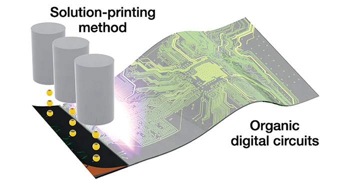
Printed Organic Digital Circuits and Its Applications

Jing Zhang1, Xiaotao Zhang1, Xiaochen Ren1,*(), Wenping Hu1,*()   

  1. 1 Tianjin Key Laboratory of Molecular Optoelectronic Sciences, Department of Chemistry, Tianjin University,Tianjin 300072, China
  • Received: Revised: Online: Published:
  • Contact: Xiaochen Ren, Wenping Hu
  • Supported by:
    The work was supported the National Key R&D Programs(2017YFA0204503); The work was supported the National Key R&D Programs(2016YFB0401100); the National Natural Science Foundation of China(91833306); the National Natural Science Foundation of China(51633006); the National Natural Science Foundation of China(51703159); the National Natural Science Foundation of China(51703160); the National Natural Science Foundation of China(51733004)
Richhtml ( 40 ) PDF ( 705 ) Cited
Export

EndNote

Ris

BibTeX

Printed organic electronic technology is the electronic manufacturing technology based on the printing method, and particularly refers to the printing of electronic devices by using functional inks consisting of organic semiconductor materials. The development of this technology involves multidisciplinary approaches including material chemistry and microelectronics. The unique fabrication method and device form brings the flexibility, low-cost and large-area processability to the devices, complementary to Si based electronics in the applications of biosensing, electronic skin and flexible display. To capture the rapid progress of this research field, a timely review of recent work is necessary. In addition, a better understanding of both material processing and digital electronics is essential for the development of this field. In this work, we provide a comprehensive overview from the perspective of printing technology and circuit systems. Printing technologies such as inkjet printing, screen printing, and transfer printing, including both the printing mechanisms and their applications related to organic devices are introduced. The functionality and the development challenge of organic digital circuits such as inverter, NAND gate, ring oscillator and D-type flip-flop, are summarized. We then review the applications of printed organic electronics, such as RFID, electronic skin, and OLED displays. Finally, the challenges and the outlook of printed organic electronics are briefly discussed.

Contents

1 Introduction

2 Printing Technology

2.1 Printing methods

2.2 Printed electronics

3 Organic digital circuit

3.1 Inverter

3.2 NAND

3.3 Ring oscillator

3.4 D?Flip?flop

4 Applications

4.1 RFID tag

4.2 Electronic Skin

4.3 OLED display

5 Conclusion and outlook

Fig.1 (a) Traditional silicon-based electronic products[10](b) Printed electronic products attached to the skin[11]
Fig.2 Schematic diagram of the inkjet printing[18]
Fig.3 Schematic diagram of the screen printing[22]
Fig.4 (a) Transfer printing[23],(b) gravure printing[24]
Table 1 Comparison of the features of different printing methods[28]
Fig.5 (a) Pseudo-D inverter,(b) Pseudo-E inverter[31]
Fig.6 (a) Static input-output characteristics of fifteen inverters in a fabricated array.(b) Plotted are the trip voltage(VTrip, blue solid circles) and small-signal gain(red solid triangles), as a function of VDD[35]
Fig.7 (a) Schematic circuits of a conventional NAND gate and a proposed 3D NAND gate.(b) DC VOUT-VIN characteristics of a 3D NAND gate.(c)A large-scale flexible logic circuitry implemented by using a 12×8 3D NAND gate array(scale bar is 4mm)[36]
Fig.8 Transistor density trend of printed electronics fabricated by various printing techniques[36]
Fig.9 All-printed five-stage ring oscillators with the oscillated frequency of(a) 0.7,(b) 12.2, and(c) 60 Hz at 10 V dc, and(d) 67.4 Hz at 12 V dc [50]
Fig.10 (a) A diagram showing the cross-section of the D flip-flop(DFF) circuit.(b) A photographic image of the CMOS device, including six DFF circuits and two selector circuits. Both p-type and n-type crystals were grown in the areas surrounded by dotted lines.(c) The input(CLOCK and DATA) and output(Q and NQ) signals of a typical DFF circuit fabricated on aluminum oxide[32]
Fig.11 (a) Schematic circuit diagram for 13.56-MHz-operated 1-bit RF tag[50],(b) Block diagram of hybrid RFID tag[59],(c) Block diagram of the 13.56-MHz RFID tag and PWM coding scheme,(d)Photo of the RFID tag foil bonded to flexible flat cables[60]
Fig.12 The need to cover 3-D surface of(a) and(b) robot’s body and(c) prosthetic limbs with a large number of touch sensors has been a key driver for application for flexible and conformable e-skin.(d) E-skin is now being used to develop wearable patches(or “second skin”) with sensors for health monitoring[63]
Fig.13 (a) At only 2 μm thickness, our devices are ultraflexible and can be crumpled like a sheet of paper. Scale bar, 1 cm.(b) Tactile sensor sheet tightly conforming to a model of the human upper jaw. Scale bar, 1 cm. [66](c) Image and circuit schematic of a model hand with DiTact sensors on the fingertips connected with stretchable interconnects.[67](d) Introduction to the biomedical application of AMF-mediated LM e-skin with a bioelectromagnetic thermal effect to spatiotemporally control wireless multisite tumor treatment[67]
Fig.14 (a)Images of AMOLED panel driven by the printed OTFT-backplane[68].(b)The structure of the OLEDs and the luminance according to the applied voltage[69].(c) A physical photo of a full-color QD-OLED display with a size of 6.6 inches[70]
[1]
Xu Y, Liu C, Khim D, Noh Y Y. Phys. Chem. Chem. Phys., 2015, 17(40):26553.
[2]
Zhu B W, Gong S, Lin F G, Wang Y, Ling Y Z, An T C, Cheng W L. Adv. Electron. Mater., 2019, 5(1):1800509.
[3]
Bucella S G, Luzio A, Gann E, Thomsen L, McNeill C R, Pace G, Perinot A, Chen Z H, Facchetti A, Caironi M. Nat. Commun., 2015, 6:8394.
[4]
Lin Z Y, Liu Y, Halim U, Ding M N, Liu Y Y, Wang Y L, Jia C C, Chen P, Duan X D, Wang C, Song F, Li M F, Wan C Z, Huang Y, Duan X F. Nature, 2018, 562(7726):254.
[5]
Yu Y, Xiao X, Zhang Y K, Li K, Yan C, Wei X L, Chen L N, Zhen H Y, Zhou H, Zhang S D, Zheng Z J. Adv. Mater., 2016, 28(24):4926.
[6]
Wang D R, Zhang Y K, Lu X, Ma Z J, Xie C, Zheng Z J. Chem. Soc. Rev., 2018, 47(12):4611.
[7]
Lee T Y, Choi T M, Shim T S, Frijns R A M, Kim S H. Lab a Chip, 2016, 16(18):3415.
[8]
Kim S H, Hong K, Xie W, Lee K H, Zhang S P, Lodge T P, Frisbie C D. Adv. Mater., 2013, 25(13):1822.
[9]
Zi W, Jin Z W, Liu S Z, Xu B M. J. Energy Chem., 2018, 27(4):971.
[10]
Jayesh S, Elias J. Int. J. Simul. Multidisci. Des. Optim., 2019, 10:A11.
[11]
Kim D H, Lu N, Ma R, Kim Y S, Kim R H, Wang S, Wu J, Won S M, Tao H, Islam A, Yu K J. Science, 2011, 333:838.
[12]
Sirringhaus H, Kawase T, Friend R H, Shimoda T, Inbasekaran M, Wu W, Woo E P. Science, 2000, 290(5499):2123.
[13]
Sele C W, von Werne T, Friend R H, Sirringhaus H. Adv. Mater., 2005, 17(8):997.
[14]
Wang C L, Dong H L, Jiang L, Hu W P. Chem. Soc. Rev., 2018, 47(2):422.
[15]
Fu B B, Wang C, Sun Y T, Yao J R, Wang Y, Ge F Y, Yang F X, Liu Z Y, Dang Y F, Zhang X T, Shao X F, Li R J, Hu W P. Adv. Mater., 2019, 31(35):1970251.
[16]
Wang S M, Yao S S, Lin J S, Xia G D. Ceram. Int., 2019, 45(8):9829.
[17]
Ante F, Kälblein D, Zaki T, Zschieschang U, Takimiya K, Ikeda M, Sekitani T, Someya T, Burghartz J N, Kern K, Klauk H. Small, 2012, 8(1):73.
[18]
Kang B, Lee W H, Cho K. ACS Appl. Mater. Interfaces, 2013, 5(7):2302.
[19]
Duineveld P C. J. Fluid Mech., 2003, 477:175.
[20]
Lim J, Lee W, Lee H, Lee J, Park Y, Cho K. Adv. Funct. Mater., 2008, 18(2):229.
[21]
Fukuda K, Takeda Y, Mizukami M, Kumaki D, Tokito S. Sci. Rep., 2014, 4:3947.
[22]
Duan S M, Gao X, Wang Y, Yang F X, Chen M X, Zhang X T, Ren X C, Hu W P. Adv. Mater., 2019, 31(16):1807975.
[23]
Carlson A, Bowen A M, Huang Y G, Nuzzo R G, Rogers J A. Adv. Mater., 2012, 24(39):5284.
[24]
Sung D, de la Fuente Vornbrock A, Subramanian V. IEEE Trans. Comp. Packag. Technol., 2010, 33(1):105.
[25]
Meitl M A, Zhu Z T, Kumar V, Lee K J, Feng X, Huang Y Y, Adesida I, Nuzzo R G, Rogers J A. Nat. Mater., 2006, 5(1):33.
[26]
de la Fuente Vornbrock A, Sung D, Kang H, Kitsomboonloha R, Subramanian V. Org. Electron., 2010, 11(12):2037.
[27]
Feng X, Meitl M A, Bowen A M, Huang Y G, Nuzzo R G, Rogers J A. Langmuir, 2007, 23(25):12555.
[28]
Fukuda K, Someya T. Adv. Mater., 2017, 29(25):1602736.
[29]
Khim D, Luzio A, Bonacchini G E, Pace G, Lee M J, Noh Y Y, Caironi M. Adv. Mater., 2018, 30(20):1705463.
[30]
Takeda Y, Hayasaka K, Shiwaku R, Yokosawa K, Shiba T, Mamada M, Kumaki D, Fukuda K, Tokito S. Sci. Rep., 2016, 6:25714.
[31]
Shao L L, Chu T Y, Tao Y, Cheng K T. 2018 International Flexible Electronics Technology Conference(IFETC). IEEE, 2018, 8584012.
[32]
Yamamura A, Matsui H, Uno M, Isahaya N, Tanaka Y, Kudo M, Ito M, Mitsui C, Okamoto T, Takeya J. Adv. Electron. Mater., 2017, 3(7):1600456.
[33]
Kjellander B K C, Smaal W T T, Myny K, Genoe J, Dehaene W, Heremans P, Gelinck G H. Org. Electron., 2013, 14(3):768.
[34]
Dell’Erba G, Luzio A, Natali D, Kim J, Khim D, Kim D Y, Noh Y Y, Caironi M. Appl. Phys. Lett., 2014, 104(15):153303.
[35]
Shiwaku R, Takeda Y, Fukuda T, Fukuda K, Matsui H, Kumaki D, Tokito S. Sci. Rep., 2016, 6:34723.
[36]
Kwon J, Takeda Y, Shiwaku R, Tokito S, Cho K, Jung S. Nat. Commun., 2019, 10:54.
[37]
Almansouri A S, Ouda M H, Salama K N. IEEE Trans. Microwave Theory Techn., 2018, 66(5):2409.
[38]
Tokito S. 2018 International Flexible Electronics Technology Conference(IFETC). IEEE, 2018, 8583876.
[39]
Bebiche S, Bouhadda I, Mohammed-Brahim T, Coulon N, Bergamini J F, Poriel C, Jacques E. Solid-State Electron., 2017, 130:49.
[40]
Klauk H, Zschieschang U, Pflaum J, Halik M. Nature, 2007, 445(7129):745.
[41]
Cho S I, Mizukami M. J. Korea Inst. Electron. Commun. Sci., 2019, 14:87.
[42]
Elsobky M, Elattar M, Alavi G, Letzkus F, Richter H, Zschieschang U, Strecker M, Klauk H, Burghartz J N. Org. Electron., 2017, 50:491.
[43]
Hayasaka K, Matsui H, Takeda Y, Shiwaku R, Tanaka Y, Shiba T, Kumaki D, Tokito S. Adv. Electron. Mater., 2017, 3(9):1700208.
[44]
Chartier I, Jacob S, Charbonneau M, Aliane A, Plihon A, Coppard R, Gwoziecki R, Verilhac J M, Serbutoviez C, Dhez O, Cantatore E, Domingues dos Santos F. 2014 44th European Solid State Device Research Conference(ESSDERC). IEEE, 2014, 6948795.
[45]
Myny K, van Veenendaal E, Gelinck G H, Genoe J, Dehaene W, Heremans P. 2011 IEEE International Solid-State Circuits Conference. IEEE, 2011, 5746337.
[46]
Zschieschang U, Kang M J, Takimiya K, Sekitani T, Someya T, Canzler T W, Werner A, Blochwitz-Nimoth J, Klauk H. J. Mater. Chem., 2012, 22(10):4273.
[47]
Ji D Y, Jiang L, Dong H L, Meng Q, Zhen Y G, Hu W P. J. Mater. Chem. C, 2014, 2(21):4142.
[48]
Ogier S D, Matsui H, Feng L R, Simms M, Mashayekhi M, Carrabina J, TerÉs L, Tokito S. Org. Electron., 2018, 54:40.
[49]
Janneck R, Nowack T S, de Roose F, Ali H, Dehaene W, Heremans P, Genoe J, Rolin C. Org. Electron., 2019, 67:64.
[50]
Jung M, Kim J, Noh J, Lim N, Lim C, Lee G, Kim J, Kang H, Jung K, Leonard A D, Tour J M, Cho G. IEEE Trans. Electron Devices, 2010, 57(3):571.
[51]
Takeda Y, Yoshimura Y, Adib F A E B, Kumaki D, Fukuda K, Tokito S. Jpn. J. Appl. Phys., 2015, 54(4S):04DK03.
[52]
De Ruiter G, Motiei L, Choudhury J, Oded N, Van der Boom M. Angewandte Chemie Int. Ed., 2010, 49(28):4780.
[53]
Uno M, Kanaoka Y, Cha B S, Isahaya N, Sakai M, Matsui H, Mitsui C, Okamoto T, Takeya J, Kato T, Katayama M, Usami Y, Yamakami T. Adv. Electron. Mater., 2015, 1(12):1500178.
[54]
Myny K. Nat. Electron., 2018, 1(1):30.
[55]
Siegel A C, Phillips S T, Dickey M D, Lu N S, Suo Z G, Whitesides G M. Adv. Funct. Mater., 2010, 20(1):28.
[56]
Yamamura A, Watanabe S, Uno M, Mitani M, Mitsui C, Tsurumi J, Isahaya N, Kanaoka Y, Okamoto T, Takeya J. Sci. Adv., 2018, 4(2):eaao5758.
[57]
Myny K, Steudel S, Vicca P, Furthner F, van der Putten B, Tripathi A K, Gelinck G H, Genoe J, Dehaene W, Heremans P. Org. Electron., 2010, 11:1176.
[58]
Myny K, Steudel S, Vicca P, Beenhakkers M J, van Aerle N A J M, Gelinck G H, Genoe J, Dehaene W, Heremans P. Solid-State Electron., 2009, 53(12):1220.
[59]
Myny K, RockelÉ, M, Chasin A, Pham D V, Steiger J, Botnaras S, Weber D, Herold B, Ficker J, Van Der Putten B, Gelinck G H. IEEE Trans. Electron Devices, 2014, 61:2387.
[60]
Fiore V, Battiato P, Abdinia S, Jacobs S, Chartier I, Coppard R, Klink G, Cantatore E, Ragonese E, Palmisano G. IEEE Trans. Circuits Syst. I: Regul. Pap., 2015, 62(6):1668.
[61]
Dahiya R S, Mittendorfer P, Valle M, Cheng G, Lumelsky V J. IEEE Sensor J., 2013, 13(11):4121.
[62]
Núñez C G, Navaraj W T, Polat E O, Dahiya R. Adv. Funct. Mater., 2017, 27(18):1606287.
[63]
Dahiya R. Proc. IEEE, 2019, 107(2):247.
[64]
Chortos A, Liu J, Bao Z N. Nat. Mater., 2016, 15(9):937.
[65]
Kaltenbrunner M, Sekitani T, Reeder J, Yokota T, Kuribara K, Tokuhara T, Drack M, Schwödiauer R, Graz I, Bauer-Gogonea S, Bauer S, Someya T. Nature, 2013, 499(7459):458.
[66]
Tee B C K, Chortos A, Berndt A, Nguyen A K, Tom A, McGuire A, Lin Z C, Tien K, Bae W G, Wang H, Mei P, Chou H H, Cui B, Deisseroth K, Ng T N, Bao Z. Science, 2015, 350(6258):313.
[67]
Wang X L, Fan L L, Zhang J, Sun X Y, Chang H, Yuan B, Guo R, Duan M H, Liu J. Adv. Funct. Mater., 2019, 29(51):1907063.
[68]
Ryu G S, Kim J S, Jeong S H, Song C K. Org. Electron., 2013, 14(4):1218.
[69]
Kim J S, Song C K. Org. Electron., 2016,30∶45.
[70]
Hu Z P, Yin Y M, Ali M U, Peng W X, Zhang S J, Li D Z, Zou T Y, Li Y Y, Jiao S B, Chen S J, Lee C Y, Meng H, Zhou H. Nanoscale, 2020, 12(3):2103.
[1] Cui Shuyuan, Liu Jun, Wu Wei. Preparation of Metal Nanoparticles-Based Conductive Inks and Their Applications in Printed Electronics [J]. Progress in Chemistry, 2015, 27(10): 1509-1522.