


1 引言
2 二维磁性纳米材料的分类
2.1 诱导产生的磁性二维纳米材料
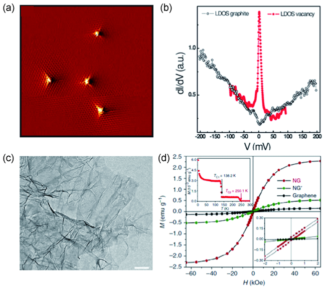
图1 (a) 氩离子轰击之后石墨表面的STM图像; (b) 在6 K测试条件下,石墨表面和碳空位处的dI/dV谱[31];(c) 超掺杂技术制备的高氮含量石墨烯的TEM图像;(d) 2 K条件下,未掺杂石墨烯、未经氟化处理氮掺杂的石墨烯以及使用超掺杂技术制备的高氮含量石墨烯的M-H曲线[32]Fig.1 (a) STM image of the graphite surface after treatment of Ar+ ion irradiation; (b) The dI/dV spectra measured on the pristine graphite surface and top of the single C vacancy at 6 K[31]; Copyright 2010, American Physical Society. (c) TEM image of superdoped graphene with a high level of N; (d) M-H curves of pristine graphene, N doped graphene without fluorination pretreatment and superdoped graphene measured at 2 K[32]. Copyright 2016, Springer Nature |
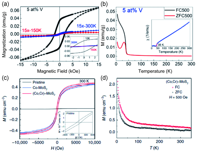
图2 (a) 5 at% V掺杂MoS2纳米片在不同温度下的M-H曲线;(b) 5 at% V掺杂MoS2纳米片的场冷-零场冷曲线[33]; (c) 单层未掺杂的MoS2, Co掺杂的MoS2以及Co、Cr共掺杂的MoS2在300 K下的M-H曲线;(d) 单层Co、Cr共掺杂MoS2的场冷-零场冷曲线[34]Fig.2 (a) M-H curves of 5 at% V doped MoS2 nanosheets at different temperatures; (b) FC-ZFC curves of 5 at% V doped MoS2 nanosheets[33]; Copyright 2017, American Chemical Society. (c) M-H curves of monolayer pristine MoS2, Co-MoS2 and (Co, Cr)-MoS2 measured at 300 K; (d) FC-ZFC curves of monolayer (Co, Cr)-MoS2[34]. Copyright 2019, Springer Nature |
2.2 具有本征磁性的二维纳米材料
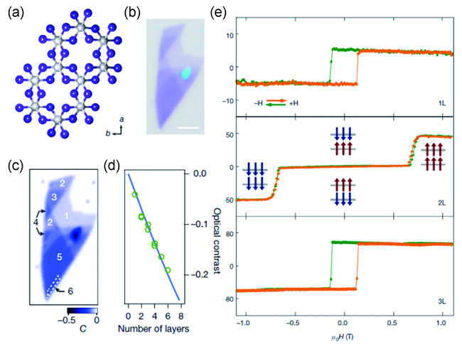
图3 (a) CrI3的晶体结构; (b) 剥离得到的CrI3纳米片的光学显微镜图像; (c) 计算得到的该纳米片的光学衬度图; (d) 不同层厚CrI3的平均光学衬度(绿色圈)按照菲涅尔公式拟合(蓝色直线); (e) 一层、两层以及三层CrI3的磁光克尔信号[8]Fig.3 (a) The crystal structure of CrI3; (b) Optical image of the exfoliated CrI3 nanoflake; (c) The calculated optical contrast map of this exfoliated CrI3 nanoflake; (d) The average optical contrast of the CrI3 with different thickness (the green circles) fitted by Fresnel’s equations (the blue line); (e) MOKE signals of monolayer, bilayer and trilayer CrI3[8]. Copyright 2017, Springer Nature |

图4 (a) 剥离得到Cr2Ge2Te6的光学显微镜图像及该区域在不同温度下的克尔转角成像; (b) 6层厚度Cr2Ge2Te6的克尔转角随磁场的变化曲线及从不同方向扫描且B=0时的克尔转角成像[9]Fig.4 (a) Optical image of the exfoliated Cr2Ge2Te6 nanoflake and the Kerr rotation images of this area at different temperatures; (b) Hysteresis loop of the six-layer Cr2Ge2Te6 and the Kerr rotation images at zero field after varying the field from different direction[9]. Copyright 2017, Springer Nature |
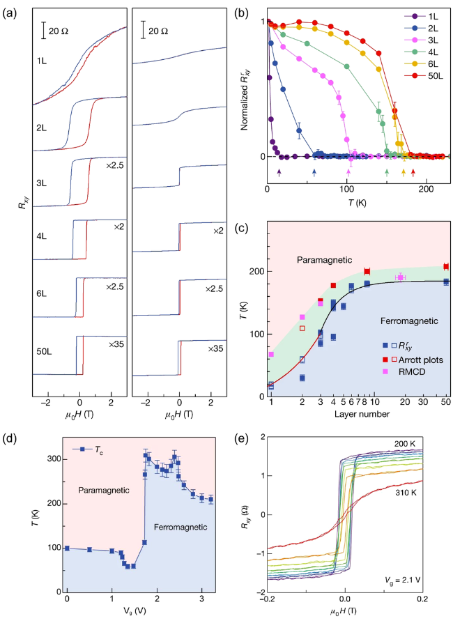
图5 (a) 不同厚度Fe3GeTe2的霍尔电阻随外磁场的变化关系(左侧: 低温,右侧: 100 K); (b) 不同厚度Fe3GeTe2的剩余霍尔电阻随温度的变化关系曲线; (c) 磁转变温度和Fe3GeTe2层数之间的相图; (d) 三层Fe3GeTe2的居里温度与外加电压之间的相图; (e) 在2.1 V外加电压,不同温度条件下,四层厚度Fe3GeTe2的霍尔电阻随磁场的变化关系[43]Fig.5 (a) Hysteresis loop of the Hall resistance of Fe3GeTe2 with different thicknesses (left: at low temperature, right: at 100 K); (b) Remanent anomalous Hall resistance of Fe3GeTe2 with different thicknesses as a function of temperature; (c) The phase diagram of Fe3GeTe2 with varied thicknesses and temperatures; (d) The phase diagram of trilayer Fe3GeTe2 with varied gate voltages and temperatures; (e) Hysteresis loop of the Hall resistance of four-layer Fe3GeTe2 under different temperatures and a gate voltage of 2.1 V[43]. Copyright 2018, Springer Nature |
3 二维磁性纳米材料的制备方法
3.1 机械剥离法
3.2 电化学剥离法
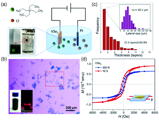
图6 (a) 电化学剥离VSe2的装置示意图;(b)在SiO2/Si衬底上的超薄VSe2纳米片的显微镜图像;(c) 剥离得到的VSe2纳米片的厚度和尺寸的统计直方图;(d) 超薄VSe2纳米片在10 K和300 K下的M-H曲线[55]Fig.6 (a) Schematic diagram of the electrochemical exfoliation setup for VSe2; (b) Optical images of ultrathin VSe2 nanoflakes on SiO2/Si substrate; (c) Statistical histograms for the thickness and lateral size distributions of the exfoliated ultrathin VSe2 nanoflakes; (d) the M-H curves of the ultrathin VSe2 nanoflakes at 10 K and 300 K[55]. Copyright 2019, Wiley-VCH |
3.3 超声辅助液相剥离法
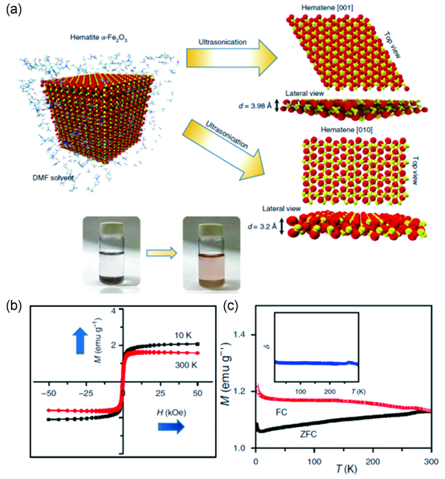
图7 (a) 超声辅助液相剥离法制备超薄铁磁性的α-Fe2O3纳米片示意图; (b) 超薄铁磁性α-Fe2O3纳米片在10 K和300 K下的M-H曲线; (c) 超薄铁磁性α-Fe2O3纳米片在1000 Oe磁场下的场冷-零场冷曲线[59]Fig.7 (a) Schematic diagram of sonication-assisted liquid-phase exfoliation for ultrathin ferromagnetic α-Fe2O3 nanosheets; (b) M-H curves of the ultrathin ferromagnetic α-Fe2O3 nanosheets at 10 K and 300 K; (c) FC-ZFC curves of ultrathin ferromagnetic α-Fe2O3 nanosheets at 1000 Oe[59]. Copyright 2018, Springer Nature |
3.4 化学气相沉积法

图8 (a) 金属性的MTe2 (M=V, Nb, Ta)纳米片的合成制备示意图; (b) MTe2 (M=V, Nb, Ta)的原子力显微镜图像; (c) MTe2 (M=V, Nb, Ta)在10 K下的M-H曲线[10]Fig.8 (a) Schematic diagram of the synthesis of ultrathin metallic MTe2 (M=V, Nb, Ta) nanoplates; (b) AFM images of ultrathin MTe2 (M=V, Nb, Ta) nanoplates; (c) M-H curves of the ultrathin MTe2 (M=V, Nb, Ta) nanoplates at 10 K[10]. Copyright 2018, Wiley-VCH |
3.5 分子束外延法

图9 (a) V5Se8的晶体结构示意图; (b) 30层厚度的V5Se8的截面扫描透射电子显微镜图像; (c) 平面晶格长度随生长时间的变化曲线; (d) 2 K温度下,不同层厚V5Se8的反常霍尔电阻率随外磁场的变化曲线; (e) 不同层厚V5Se8的饱和反常霍尔电阻率和剩余反常霍尔电阻率随温度的变化曲线[74]Fig.9 (a) Crystal structure of V5Se8; (b) The cross-sectional STEM image of 30 ML thick V5Se8film; (c) The evolution of in-plane lattice length with growth time; (d) The ρAH-μ0H curves of V5Se8 with different thicknesses at 2 K; (e) The temperature dependences of the ρAH, sat and ρAH, rem of V5Se8 with different thicknesses[74]. Copyright 2019, American Chemical Society |
3.6 液相合成方法
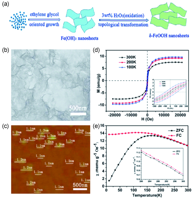
图10 (a) 二维磁性FeOOH纳米片的液相合成示意图; (b) 超薄FeOOH纳米片的TEM图像;(c) 超薄FeOOH纳米片的原子力显微镜图像;(d) 超薄FeOOH纳米片在不同温度下的磁化曲线;(e) 超薄FeOOH纳米片的场冷-零场冷曲线[77]Fig.10 (a) Schematic diagram of the synthesis of 2D magnetic FeOOH nanosheets; (b) TEM image of ultrathin FeOOH nanosheets; (c) AFM image of ultrathin FeOOH nanosheets; (d) Magnetization curves of the ultrathin FeOOH nanosheets at different temperatures; (e) FC-ZFC curves of ultrathin FeOOH nanosheets[77]. Copyright 2014, Royal Society of Chemistry |
4 二维磁性纳米材料的磁性调控
4.1 电场调控
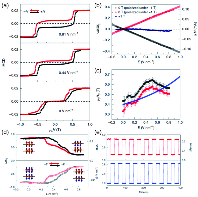
图11 (a) 双层CrI3在不同电场下的磁圆二色谱信号随磁场的变化关系; (b) 不同固定磁场下饱和磁化强度的绝对变化和相对变化值随外加电场的变化关系; (c)转变磁场随外加电场的变化关系; (d) 在0.44 T和-0.44 T下,磁化强度及归一化的磁化强度值随电场的变化曲线; (e) 通过周期性地改变电场强度调控饱和磁化强度值[79]Fig.11 (a) MCD signals of bilayer CrI3 as a function of magnetic field under different electric fields; (b) The absolute and relative changes of magnetization as a function of electric field under different fixed magnetic fields; (c) The critical magnetic fields as a function of electric field; (d) The magnetization and the normalized magnetization as a function of electric field at 0.44 T and -0.44 T, respectively; (e) Repeated changing the magnetization by applying a periodic electric field at 0.44 T[79]. Copyright 2018, Springer Nature |
4.2 静电掺杂调控
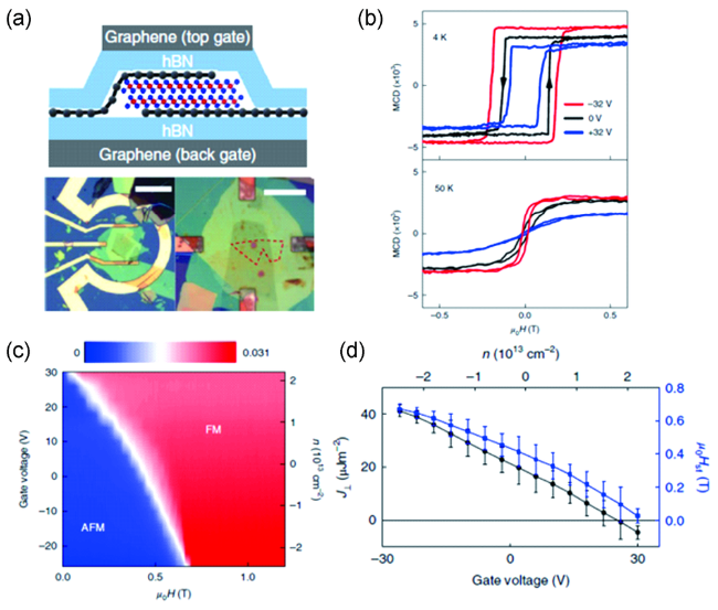
图12 (a) 基于CrI3双栅极场效应器件示意图及其光学显微镜照片; (b) 单层CrI3在不同电压和温度下的MCD信号和外加磁场之间的关系;(c) 双层CrI3的转变磁场与外加电压之间的相图;(d) 层间交换常数和转变磁场与外加电压和掺杂浓度之间的关系[80]Fig.12 (a) Schematic diagram of dual-gate CrI3 field-effect device and the optical images of the devices; (b) MCD signals as a function of magnetic field under different gate voltages and temperatures; (c) The phase diagram of bilayer CrI3 with varied magnetic field and gate voltages; (d) Interlayer exchange constant and critical magnetic fields as functions of gate voltages and doping concentration[80]. Copyright 2018, Springer Nature |
4.3 压力调控
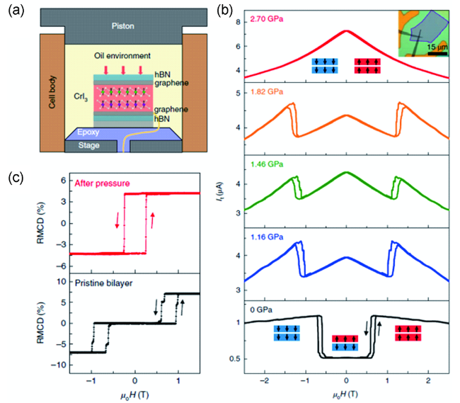
图13 (a) 施加高压装置示意图;(b) 施加不同压力时隧穿电流与磁场的关系;(c) 双层CrI3施加压力(2.45 Gpa)前后的RMCD信号[81]Fig.13 (a) Schematic diagram of high-pressure experimental set-up; (b) The tunneling current as a function of magnetic field under different pressures; (c) RMCD signals of bilayer CrI3 before and after pressure (2.45 Gpa) treatment[81]. Copyright 2019, Springer Nature |