


1 引言
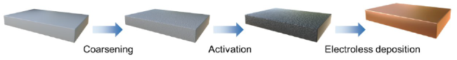
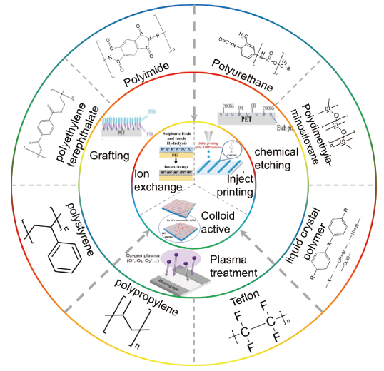
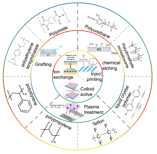
图2 电子领域中化学镀常用的基底材料和粗化、活化方法示意图。粗化:化学刻蚀、接枝、等离子体处理;活化:离子交换、墨水打印、胶体活化Fig.2 Schematic diagram of commonly used substrate materials and roughening and activation methods for electroless plating in the field of electronics. Roughening: chemical etching, grafting, plasma treatment; activation: ion exchange, ink printing, colloidal activation. |
2 聚合物化学镀原理及电子领域的应用
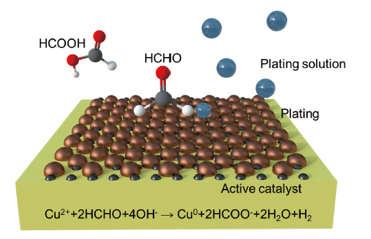
2.1 化学镀原理
2.2 导电互连
图3 (a)PCB导电互连示意图;(b)在聚合物基底上进行化学镀制备电磁屏蔽层示意图[50];(c)在元器件之上通过一层聚合物绝缘层再进行化学镀进行热量管理的示意图[51]Fig.3 (a) Schematic diagram of conductive interconnection of PCB; (b) Schematic diagram of electromagnetic shielding layer prepared by electroless plating on a polymer substrate[50]; (c) Schematic representation of heat management by electroless plating of components with a layer of polymer insulation[39] |
2.3 电磁屏蔽
2.4 散热导热
3 聚合物表面粗化方法
3.1 化学刻蚀
3.2 等离子体处理
3.3 接枝改性
4 聚合物化学镀前活化方法
4.1 催化剂金属离子吸附还原
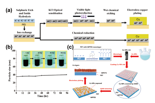
4.2 催化剂直接吸附
4.3 直接墨水书写与图案印刷
5 聚酰亚胺(PI)化学镀前处理技术
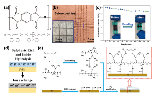
图7 (a)聚酰亚胺结构式;(b)聚酰亚胺化学镀后百格刀测试[47];(c)聚酰亚胺化学镀后弯折实验与导电性变化测试[56];(d)聚酰亚胺化学刻蚀粗化后离子交换活化流程图[1];(e)聚酰亚胺化学刻蚀和接枝粗化后再活化流程图[30]Fig.7 (a) Structural formula of polyimide; (b) 100-square-knife test after electroless polyimide plating[47]; (c) bending test and conductivity change test after electroless polyimide plating[56] ; (d) Flow chart of ion exchange activation after chemical etching and roughening of polyimide[1]; (e) Flow chart of activation after chemical etching and grafting of polyimide[30] |
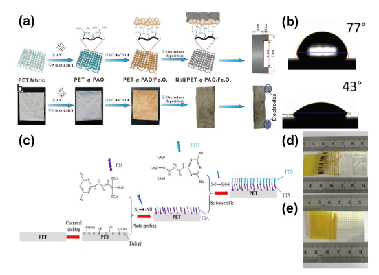
6 聚对苯二甲酸乙二酯(PET)化学镀前处理技术
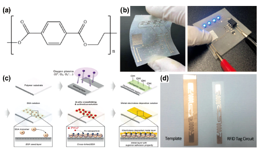
图8 (a)PET结构式;(b)PET化学镀后弯折和导电线路测试[59];(c)PET经过等离子体处理粗化后Pd催化剂直接吸附活化示意图[52];(d)PET化学镀制备的导电器件[63]Fig.8 (a) PET structural formula; (b) PET electroless plating after bending and conductive circuit test[59]; (c) Schematic diagram of direct adsorption and activation of Pd catalyst after PET roughening by plasma treatment[52]; (d) Conductive wire prepared by PET electroless plating device[72] |
表1 PI常用粗化与活化方法汇总Table 1 Summary of commonly used methods for coarsening and activation of PI |
表2 PET常用粗化与活化方法汇总Table 2 Summary of commonly used coarsening and activation methods for PET. |
| Method | Roughening reagent | Roughening conditions | Activating reagent | Activation conditions | ref |
|---|---|---|---|---|---|
| 1 | HCl | ultrasound 5 min | KH550 | / | 63 |
| AgNO3 | |||||
| PVA | |||||
| 2 | / | / | PM | Print& Plasma treatment | 62,65,66 |
| CH4N2S | |||||
| AgNO3 | |||||
| BADGE | |||||
| Hardener 593 | |||||
| 3 | Plasma treatment | / | PdCl2 | 64 | |
| 4 | MPTES | 2 h | Cuf | / | 67 |
| OAM | |||||
| Paraffin | |||||
| 5 | VTMS | 15 min | (NH4)2PdCl4 | 3min | 53 |
| METAC | 80 ℃/60 min | ||||
| MPTS |
7 聚氨酯(PU)化学镀前处理技术
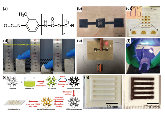
图9 (a)PU结构式;(b)PU表面化学镀制备电极[71];(c)PU导电线路最细可达28 μm[71];(d)PU海绵化学镀后弹性测试[24];(e)PU导电线路测试[71];(f)PU表面化学镀弯折实验[72];(g)PU海绵化学镀前处理流程图[72];(h)通过3D打印的PU并化学镀样品[73]Fig.9 (a) PU structural formula; (b) electrode prepared by electroless plating on PU surface[71]; (c) PU conductive line as thin as 28 μm[71]; (d) elasticity test of PU sponge after electroless plating [24]; (e) PU conductive circuit test[79]; (f) PU surface electroless plating bending experiment [80]; (g) PU sponge electroless plating pretreatment flow chart[80]; (h) 3D printed PU and electroless plating samples[82]. |
表3 PU常用粗化与活化方法汇总Table 3 Summary of commonly used coarsening and activation methods for PU |
| Method | Roughening reagent | Roughening conditions | Activating reagent | Activation conditions | ref |
|---|---|---|---|---|---|
| 1 | NaOH | 25 ℃/24 h | AgNO3 | 25 ℃/1 h | 23 |
| Dopamine | NH3·H2O | ||||
| Tris·HCl | |||||
| 2 | Tannic acid KMnO4 | 30 min | (NH4)2PdCl4 | 15 min | 69 |
| SnCl2 | |||||
| 3 | H2SO4 | / | PdCl2 | 25 ℃/10 min | 70 |
| HCl | |||||
| 4 | Na2S2O8 | 25 ℃/5 min | PdSO4 | 10 min | 72 |
| H2SO4 | |||||
| 5 | H2CrO4 | / | SnCl2 | 15 min | 71 |
| H2SO4 | HCl | ||||
| AgNO3 | |||||
| 6 | Laser irradiation | 1064 nm | / | / | 22 |
| 7 | KOH | 50 ℃/2 h | AgNO3 | 20 min | 67 |
| Laser irradiation | 460 nm/3 minn | ||||
| 8 | Chitosan | 4 h | PdCl2 | 10 min | 23 |
| NaH2PO2 | |||||
| 9 | METAC | / | (NH4)2PdCl 4 | / | 73 |
| MPTS |
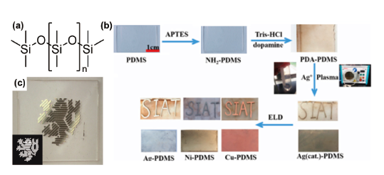
8 聚二甲氨基硅氧烷(PDMS)化学镀前处理技术
9 聚苯乙烯(PS)化学镀前处理技术
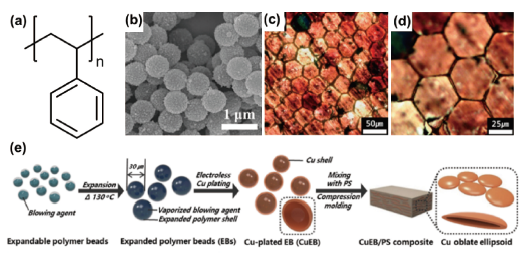
图11 (a)PS结构式;(b)PS微球化学镀铜后的SEM图[85];(c) (d)PS微球经过热压后互相接触形成导电网络[82];(e)PS微球化学镀并经过热压形成三维导电结构流程图[82]Fig.11 (a) PS structural formula; (b) SEM image of PS microspheres after electroless copper plating[85]; (c) (d) PS microspheres contacted with each other after hot pressing to form a conductive network[82]; (e) PS microspheres electroless plating and Flow chart of forming a three-dimensional conductive structure by hot pressing[82] |
10 聚丙烯(PP)化学镀前处理技术
表4 PDMS常用粗化与活化方法汇总Table 4 Summary of common coarsening and activation methods for PDMS. |
| Method | Roughening reagent | Roughening conditions | Activating reagent | Activation conditions | ref |
|---|---|---|---|---|---|
| 1 | O Plasma treatment | 10 s | AgClO4 | spin coating & UV treatment | 79 |
| MPA | |||||
| Ma-P1215 | |||||
| 2 | SnCl2 | 45 min | Ag(NH3)2NO3 | 10 min | 76 |
| C2HF3O2 | |||||
| 3 | APTES | 24 h | AgNO3 | Write& Plasma treatment | 77 |
| Tris-HCl | |||||
| Dopamine | |||||
| 4 | Alkanethiol | 3 min | PdNO3 | / | 15 |
| HNO3 | |||||
| 5 | APTMS | 12 h | Ag(NH3)2NO3 | / | 80 |
| APTES | 30 min | ||||
| 6 | APTES | 3 h | SnCl2 | / | 78 |
| Fe3O4 | |||||
| Au | |||||
表5 PS常用粗化与活化方法汇总Table 5 Summary of common coarsening and activation methods for PS |
| Method | Roughening reagent | Roughening conditions | Activating reagent | Activation conditions | ref |
|---|---|---|---|---|---|
| 1 | PVP | 70 ℃/12 h | SnCl2 | 45 ℃/40 min | 81 |
| styrene monomer | Na2SnO3 | ||||
| PdCl2 | |||||
| HCl | |||||
| 2 | NaOH | 5 min | Pd/Sn | / | 82,84 |
| 3 | H2SO4 | 40 ℃/4 h | SnCl2 | / | 85 |
| HCl | |||||
| AgNO3 | |||||
| NH4OH | |||||
| C4H4O6KNa | |||||
| 4 | FeCl3·6H2O | 24 h | Ag/Sn | / | 83 |
| Pyrrole-1-propionic acid monomer | |||||
| Pyrrole monomer |
表6 PP常用粗化与活化方法汇总Table 6 Summary of commonly used coarsening and activation methods for PP |
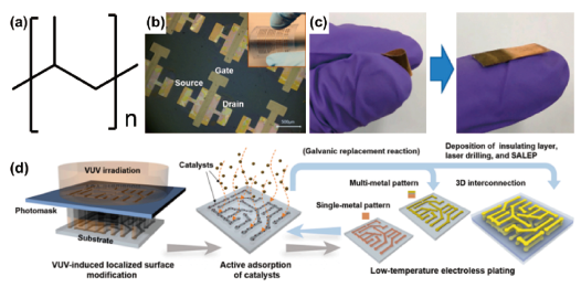
图12 (a)聚丙烯结构图;(b)聚丙烯表面化学镀制备电子器件[13];(c)聚丙烯化学镀后弯折测试[86];(d)聚丙烯在掩模板下经过紫外光照射粗化,然后使用催化剂直接吸附活化得到精确导电图案示意图[11]Fig.12 (a) Structure diagram of polypropylene; (b) Electroless plating on polypropylene surface to prepare electronic devices[13]; (c) Bending test of polypropylene after electroless plating[86]; (d) Polypropylene roughened by ultraviolet light under the mask, and then use the catalyst for direct adsorption activation to obtain a precise conductive pattern[11] |