


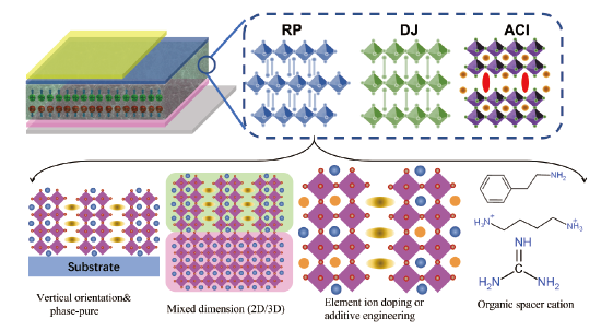
1 引言
2 二维钙钛矿的晶体结构与物理性质
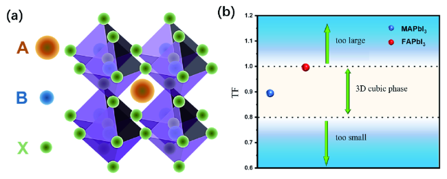
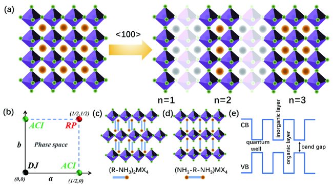
图2 (a)从3D钙钛矿<100>表面切割形成的带有有机间隔阳离子的不同n值层状钙钛矿;(b)2D钙钛矿材料的相空间图示,典型的n=1的2D层状钙钛矿结构:(c)单铵基和(d)双铵基;(e)多量子阱2D钙钛矿的能带结构Fig. 2 (a) Layered perovskite with different n values with organic spacer cations cut from 3D perovskite <100> plane. (b) Illustration of the 2D perovskite material phase space. Typical n=1 2D layered perovskite structures: (c) monoamine and (d) diamine. (e) Band structure of 2D perovskite with multiple quantum wells |
3 RP相钙钛矿
3.1 低n值2D-RP钙钛矿
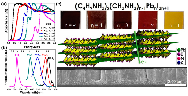
图3 不同2D钙钛矿组分的光学带隙(a)和光致发光谱(b); (c)不同n值2D钙钛矿的薄膜照片(上),(BA)2(MA)2Pb3I10的晶体取向示意图(中),以及SEM截面图(下)[31]Fig. 3 (a) Optical band gap and (b) photoluminescence spectra of different 2D perovskite; (c) images of 2D perovskite film with different N values (top), crystal orientation diagram of (BA)2(MA)2Pb3I10 (middle) and cross-sectional SEM images (bottom)[31] |
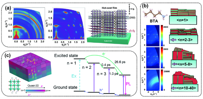
图4 (a)分别通过室温旋涂法(左)和热铸法旋涂(中)制备的(BA)2(MA)3Pb4I13 钙钛矿薄膜的掠入射广角X射线散射(GIWAXS)强度图,根据GIWAXS数据分析的沿着2D钙钛矿(111)面和(202)面的晶体取向示意图(右)[32];(b)基于BTA热铸法降维工程制备的四种不同维度尺寸区域的GIWAXS测量[33];(c)n=5钙钛矿薄膜中的载流子转移示意图,电子从小n向大n钙钛矿相转移,空穴从大n向小n钙钛矿相转移, 并且该薄膜中几乎没有n=1相[34]Fig. 4 (a) GIWAXS maps for polycrystalline room-temperature-cast (left) and hot-cast (middle) near-single-crystalline (BA)2(MA)3Pb4I13 perovskite films. Schematic representation of the (101) orientation, along with the (111) and (202) planes of a 2D perovskite crystal, consistent with the GIWAXS data (right)[32]. (b) GIWAXS measurements of hot-cast BTA-based RDPs in four different size regimes[33]. (c) Schematic of carrier transfer in the n = 5 perovskite film. The electron transfers from small-n to large-n perovskite phases, and the hole transfers from large-n to small-n perovskite phases, and there is little n = 1 phase in this thin film[34] |

图5 (a)Csx-2D钙钛矿薄膜的形貌表征(扫描电子显微镜);(b)Cs5-2D钙钛矿器件的电流密度-电压(J-V)曲线[38];(c)通过吸收光谱估算的激子结合能,2D钙钛矿显示出典型的激子峰和阶梯状的带间吸收,BA2PbI4和MA2PbI4的激子结合能分别为502 meV和153 meV[39];(d)(PPA)2(Cs/FA/MA)n-1Pbn $(I/Br)_{3_{n+1}}$ (n≤4)的GIWAXS图谱[42]Fig. 5 (a) Morphology characterization of the Csx-2D perovskite films (scanning electron microscope). (b) The current density-voltage (J-V) curve of Cs5-2D perovskite devices[38]. (c) Estimated exciton binding energy by absorption spectra. The 2D perovskites show a typical exciton peak and a step-like band-to-band absorption. The exciton binding energy of BA2PbI4 and MA2PbI4 are 502 meV and 153 meV, respectively[39]. (d) GIWAXS patterns of (PPA)2(Cs/FA/MA)n-1Pbn $(I/Br)_{3_{n+1}}$ (n ≤ 4) films[42] |
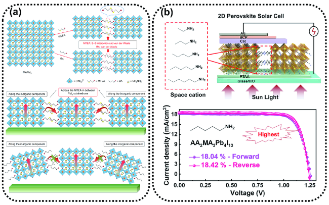
图6 (a)2D-RP钙钛矿(MTEA)2(MA)n-1Pbn 和(BA)2(MA)n-1Pbn 的晶体结构示意图以及MTEA和BA基2D钙钛矿薄膜的电荷输运示意图[43];(b)由不同有机间隔物(EA-HA)制备的2DRP钙钛矿的图示结构和最佳2D-RP PSCs(AA2MA3Pb4I13 )的J-V特性[44]Fig. 6 (a) Schematic crystal structures of the 2D-RP perovskites (MTEA)2(MA)n-1Pbn and (BA)2(MA)n-1Pbn and charge transport diagram of MTEA and BA based 2D perovskite films[43]. (b) Illustrated structures of RP-phase two-dimensional (2DRP) perovskites integrated by different organic spacers (EA-HA) and J-V characteristics of the best 2D-RP PSC (AA2MA3Pb4I13)[44] |
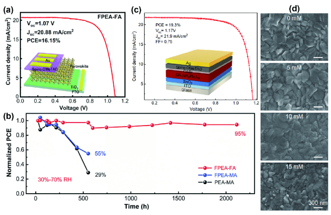
图7 (a) 性能最佳的FPEA-FA器件的电流密度-电压(J-V)曲线;插图是2D-RPP太阳能电池的器件结构;(b) 30%~70%相对湿度下未封装FPEA-FA、FPEA-MA和PEA-MA器件的归一化PCE[45];(c) 采用GABr后处理的PSCs的J-V曲线;插图是2D-RPP太阳能电池的器件结构;(d) 经不同GABr浓度处理的钙钛矿薄膜的俯视扫描电子显微镜(SEM)图像[46]Fig. 7 (a) The current density-voltage (J-V) curve of the best-performing FPEA-FA device; the inset is the device structure of the 2D-RPP solar cell. (b) The normalized PCE of unencapsulated FPEA-FA, FPEA-MA, and PEA-MA devices under 30%~70% RH[45]. (c) The J-V curve of the PSCs using GABr post-treatment; the inset is the device structure of the 2D-RPP solar cell. (d) Top-view scanning electron microscopy (SEM) images of the perovskite films treated with various GABr concentrations[46] |
3.2 高n值2D-RP 钙钛矿
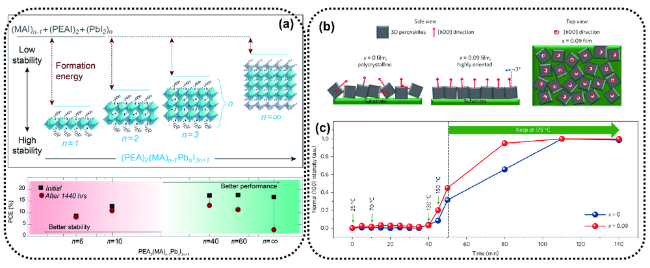
图8 (a)从2D (n=1)到3D (n=∞)具有不同n值的(PEA)2MAn-1Pbn 钙钛矿的晶胞结构(上),器件性能是n值的函数,随着n值的增加,性能得到了提高;然而,与此同时,稳定性降低(下)[47];(b)描绘了BA掺杂含量x=0.09薄膜中3D钙钛矿相的取向,与x=0薄膜相比,显示了对[h00]方向的优先取向。请注意这些方块只是示意性地说明了晶体方向,而不是真实晶粒;(c)对于两种不同的BA浓度(x=0和0.09)钙钛矿退火过程(从室温到175℃)随时间变化的稳定性[48]Fig. 8 (a) Unit cell structure of (PEA)2(MA)n-1Pbn perovskites with different n values, showing the evolution of dimensionality from 2D (n=1) to 3D (n=∞) (upper). Device performance as a function of n value, which shows that increased performance was achieved with increased n value; however, in the meantime, stability was decreased (lower)[47]. (b) Illustration depicting the orientation of the 3D perovskite phase in the x = 0.09 film, compared with a low-textured x = 0 film, showing a preference for the [h00] direction to align out-of-plane. Note that these squares just schematically illustrate the crystal orientation rather than the crystal grains. (c) Intensity of (100) reflection as a function of time during the perovskite annealing procedure (from room temperature to 175℃) for two different BA concentrations (x = 0 and 0.09)[48] |
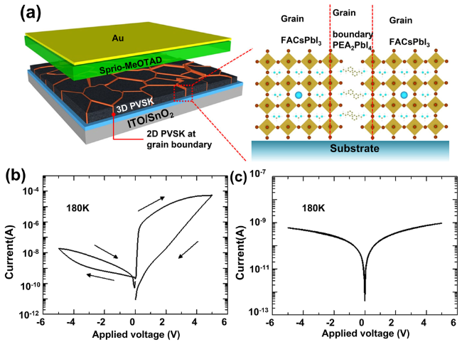
图9 (a)在晶界含有2D钙钛矿的多晶3D钙钛矿薄膜示意图;(b)在180 K条件下纯FAPbI3薄膜器件和含有1.67 mol% 2D PEA2PbI4钙钛矿器件的电流-电压(I-V)曲线[50]Fig. 9 (a) Schematics of the device incorporating polycrystalline 3D perovskite film with 2D perovskite at grain boundaries. Current-voltage (I-V) curves measured from the devices at 180 K for (b) Bare FAPbI3 film and (c) FAPbI3 film with 1.67 mol% 2D PEA2PbI4 perovskite[50] |
4 DJ相钙钛矿
4.1 非对称双铵基结构
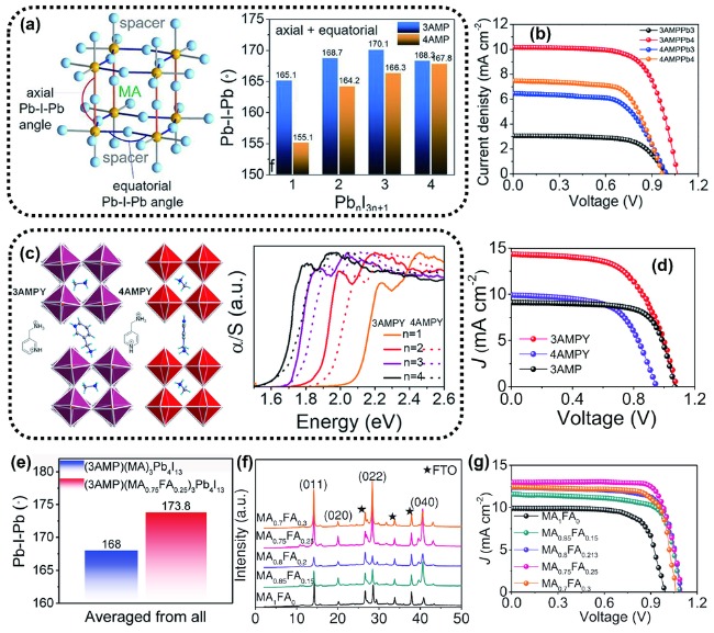
图10 (a)轴向和赤道向Pb-I-Pb角的定义以及3AMP和4AMP的平均轴向角和赤道角统计;(b)2D钙钛矿光伏器件的J-V曲线[51];(c)(3AMPY)(MA)Pb2I7和(4AMPY)(MA)Pb2I7晶体结构的侧视图和顶视图以及不同n值的两种钙钛矿的光吸收光谱;(d)相应器件的J-V曲线[52];(e)Pb-I-Pb的平均角;(f)(3AMP)(MA1-xFAx)3Pb4I13(x=0~0.3)薄膜的XRD图谱;(g)(3AMP)(MA1-xFAx)3Pb4I13 (x=0~0.3)器件的J-V特性曲线[53]Fig. 10 (a) Definition of axial and equatorial Pb-I-Pb angles and statistics of average axial and equatorial angles of 3AMP and 4 AMP. (b) J-V curves of the 2D perovskite solar cell devices[51]. (c) The side and top view of (3AMPY)(MA)Pb2I7 and (4AMPY)(MA)Pb2I7 and the optical absorption spectra of two perovskites with different n values. (d) J-V curves for the corresponding devices[52]. (e) averaged Pb-I-Pb angles. (f) XRD patterns of (3AMP)(MA1-xFAx)3Pb4I13 (x=0~0.3) films. (g) J-V curves of (3AMP)(MA1-xFAx)3Pb4I13 (x=0~0.3) devices[53] |
4.2 对称双铵基结构

图11 (a)RP和DJ相2D层状钙钛矿示意图[55];(b)晶体(101)面的方位角变化示意图[57];(c)原始器件和改性器件的电荷传输模型示意图(上)以及对应薄膜的光致发光呈现不同载流子寿命的分布(下)[58];(d)不同器件的J-V曲线[59]Fig. 11 (a) Schematic Illustration of RP and DJ Phase 2D Layered Perovskites[55]. (b) The schematic of azimuth angle evolution of (101) crystallographic[57]. (c) Schematic diagram of morphology and charge transport model of the control and target devices (up) and PL occurs distribution of different carrier lifetime for the corresponding films (down)[58]. (d) J-V curves of different devices[59] |
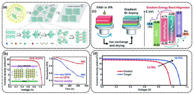
图12 (a)在FACl辅助下2D钙钛矿薄膜的微观生长机制的示意图[61];(b)最优器件的J-V曲线和未封装器件在黑暗中60℃老化的热稳定性[62];(c)通过I-和Br-之间的离子交换反应进行的梯度溴掺杂技术(GBD)来制备(BDA)FA4Pb5I16-xBrx薄膜的过程示意图和不同PSCs器件能级图示意图;(d)不同器件的J-V特性曲线[63]Fig. 12 (a) Schematic illustration depicting the microscopic growth mechanism of the 2D perovskite film under the assistance of FACl[61]. (b) J-V curves of the champion devices and thermal stability of the unencapsulated control and target devices aged at 60℃ in the dark[62]. (c) Schematic illustration of preparation process of (BDA)FA4Pb5I16-xBrx with GBD formed via the ion exchange reaction between I- and Br- and energy level diagram of PSCs based on the control and target perovskite films. (d) J-V curves of the champion control and target devices[63] |
5 ACI相钙钛矿
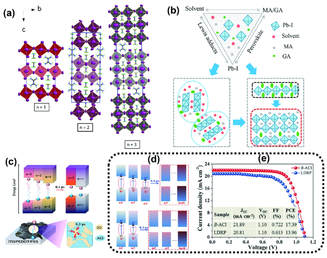
图13 (a)(GA)(MA)nPbn (n=1~3)的晶胞单元视图(突出了钙钛矿层之间GA和MA阳离子的有序晶体堆积)[64];(b)ACI型钙钛矿自组装的模型示意图[65];(c)从小n相到大n相的载流子分布以及从ACI钙钛矿中提取载流子的示意图[66];(d)混合钙钛矿量子阱的能带结构示意图和载流子传输路径。(BA)2MA2Pb3I10薄膜实现阶梯传输(上),而(BEA)0.5MA3Pb3I10薄膜具有平坦传输的途径(下);(e)以(BEA)0.5Cs0.15(FA0.83MA0.17)2.85Pb3(I0.83Br0.17)10和(BA)2Cs0.1(FA0.83MA0.17)1.9Pb3(I0.83Br0.17)10为活性层的B-ACI和LDRP钙钛矿型器件的J-V曲线[67]Fig. 13 (a) View of the unit cells of the (GA)(MA)nPbn (n = 1~3) perovskites along the crystallographic a-axis highlighting the ordered crystal packing of the GA and MA cations between the perovskite layers[64]. (b) Schematic model illustrating the self-assembly of the ACI perovskite[65]. (c) Schematics of the charge carrier localization from small n to large n phases and the charge carrier extraction from the ACI perovskite[66]. (d) Schematic of the band structure for mixed perovskite QWs and carrier transport pathway. (BA)2MA2Pb3I10 film enables a stepped transmission (up), while there is a flat transmission for (BEA)0.5MA3Pb3I10 films (down). (e) J-V curves of B-ACI and LDRP perovskite solar cells with (BEA)0.5Cs0.15(FA0.83MA0.17)2.85Pb3(I0.83Br0.17)10 and (BA)2Cs0.1(FA0.83MA0.17)1.9Pb3(I0.83Br0.17)10 as the active layer[67] |
6 结论与展望
附录
表1 不同类型2D PSCs的光伏性能参数Table 1 Photovoltaic performance parameters of different types of 2D PSCs |
| Type | 2D organic spacer cation | 2D perovskite | Voc(V) | Jsc(mA/cm2) | FF(%) | PCE(%) | ref | |
|---|---|---|---|---|---|---|---|---|
| RP |  | (PEA)2(MA)2Pb3I10 | 1.18 | 6.72 | 60 | 4.73 | 13 | |
| RP |  | (BA)2(MA)2Pb3I10 | 0.929 | 9.42 | 46 | 4.02 | 31 | |
| RP |  | (BA)2(MA)3Pb4I13 | 1.01 | 16.76 | 74.13 | 12.51 | 32 | |
| RP | 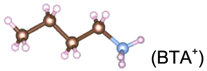  | BTA-MAPbI3 PEA-MAPbI3 | 33 | |||||
| RP |  | PEA2MAn-1PbnI3n+1 | 34 | |||||
| RP |  | PEA2MA4Pb5I16 (Vacuum polarization treatment) | 1.223 | 17.91 | 82.4 | 18.04 | 35 | |
| RP |  | (BA)2(MA0.95Cs0.05)3Pb4I13/(BrB-PEDOT:PSS) | 1.11 | 17.08 | 72.5 | 13.74 | 36 | |
| RP |  | BA2MA3Pb4I13 (DMF/DMSO) | 1.10 | 14.2 | 71 | 11.1 | 37 | |
| RP | 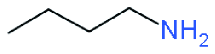 | (BA)2(MA)3Pb4I13(Cs+ doping) | 1.08 | 19.95 | 63.47 | 13.68 | 38 | |
| RP |  | MA2PbI4 | 1.06 | 21.00 | 76 | 16.92 | 39 | |
| RP | 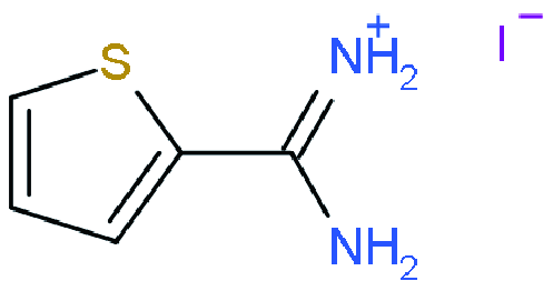 | (ThFA)2MA2PbnI10 | 1.05 | 20.17 | 79 | 16.72 | 41 | |
| RP | 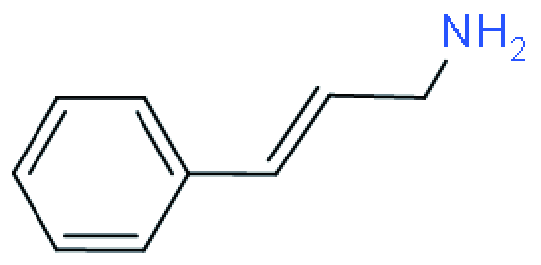 | (PPA)2(Cs0.05(FA0.88MA0.12)0.95)3 Pb4(I0.88Br0.12)13 | 1.14 | 19.33 | 67 | 14.76 | 42 | |
| RP | 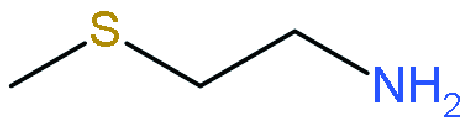 | (MTEA)2(MA)4Pb5I16 | 1.088 | 21.77 | 76.27 | 18.06 | 43 | |
| RP | 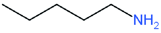 | (AA)2MA3Pb4I13 | 1.13 | 18.20 | 76.86 | 15.78 | 44 | |
| RP | 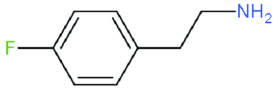 | (FPEA)2(FA)8Pb9I28 | 1.07 | 20.88 | 72.29 | 16.15 | 45 | |
| RP | 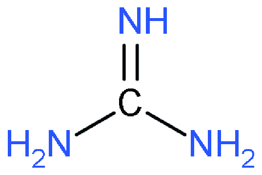 | (GA)2MA4Pb5I16 | 1.17 | 21.9 | 75 | 19.3 | 46 | |
| RP |  | PEA2MAn-1PbnI3n+1(n=60) | 1.09 | 19.12 | 73.7 | 15.36 | 47 | |
| RP | 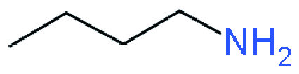 | BA0.09(FA0.83Cs0.17)0.91 Pb(I0.6Br0.4)3 | 1.18 | 19.8 | 73 | 17.2 | 48 | |
| RP | 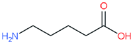 | (AVA)2PbI4@MAPbI3 | 1.06 | 22.3 | 76 | 18.0 | 49 | |
| RP | 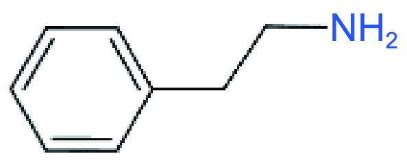 | PEA2PbI4@FA0.98Cs0.02PbI3 | 1.126 | 24.44 | 76.5 | 21.06 | 50 | |
| DJ | 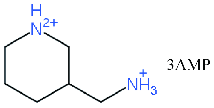 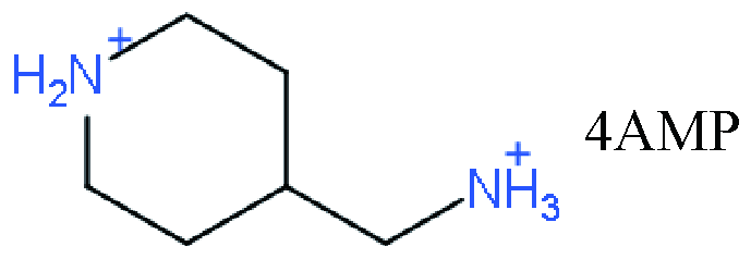 | (3AMP)(MA)3Pb4I13 | 1.06 | 10.17 | 67.6 | 7.32 | 51 | |
| DJ | 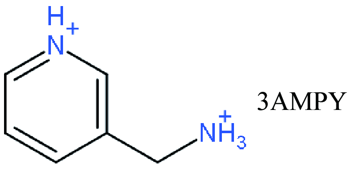 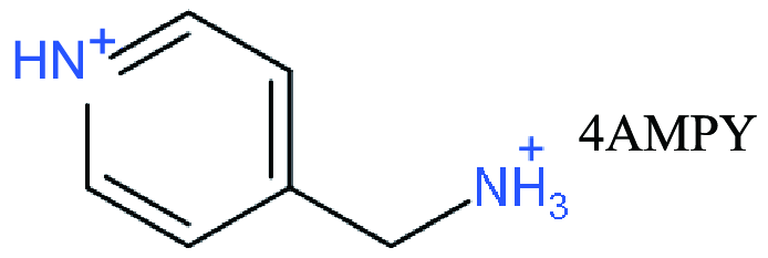 | (3AMPY)(MA)3Pb4I13 | 1.08 | 14.34 | 59.58 | 9.20 | 52 | |
| DJ | 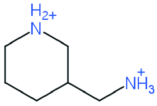 | (3AMP)(MA0.75FA0.25)3Pb4I13 | 1.09 | 13.69 | 81.04 | 12.04 | 53 | |
| DJ |  | (PDA) (MA)3Pb4I13 | 0.98 | 19.50 | 69 | 13.3 | 55 | |
| DJ |  | (BzDA)(Cs0.05MA0.15FA0.8)9Pb10(I0.93Br0.07)31 | 1.02 | 21.5 | 71 | 15.6 | 56 | |
| DJ |  | (BDA)(MA)4Pb5I16 (NH4SCN as additive) | 1.11 | 16.07 | 81.45 | 14.53 | 57 | |
| DJ |  | (ThDMA)(MA)4Pb5I16 | 1.07 | 19.55 | 75.46 | 15.75 | 58 | |
| DJ | 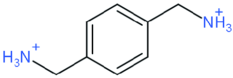 | (PDMA)(MA)3Pb4I13 | 1.15±0.025 | 21.10±0.53 | 62.58±1.5 | 15.09±0.32 | 59 | |
| DJ | 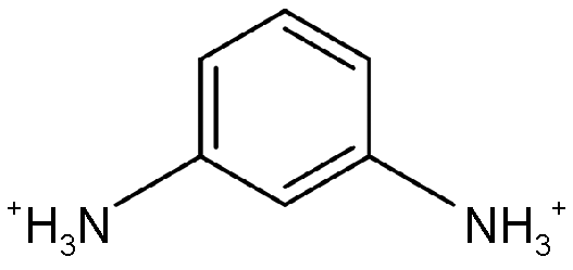 | (mPDA)MA5Pb6I19 | 0.82 | 14.74 | 51 | 6.16 | 60 | |
| DJ | 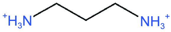 | (PDA)(FA)3Pb4I13 (FACl as additive) | 1.10 | 17.30 | 72.5 | 13.8 | 61 | |
| DJ | 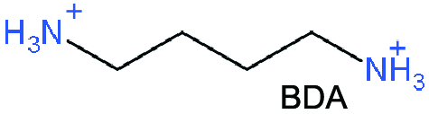 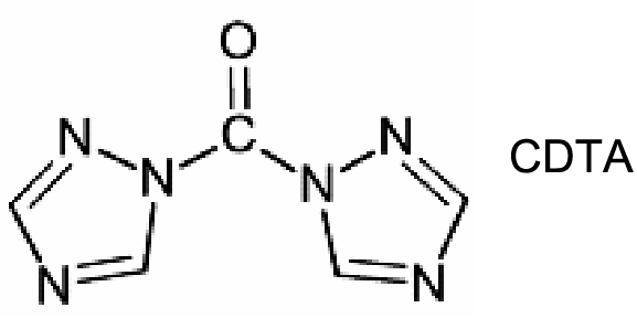 | (BDA)FA4Pb5I16 (CDTA as additive) | 1.064 | 19.71 | 76.6 | 16.07 | 62 | |
| DJ | 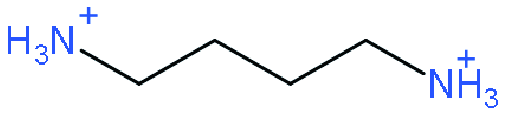 | (BDA)FA4Pb5I16-xBrx | 1.107 | 19.69 | 76.8 | 16.75 | 63 | |
| ACI |  | GAMA3Pb3I10 | 0.974 | 9.357 | 79.68 | 7.26 | 64 | |
| ACI |  | GAMA3Pb3I10 | 1.15 | 18.8 | 67.8 | 14.69 | 65 | |
| ACI |  | (GA)(MA)3Pb3I10 | 1.08 | 20.75 | 74.52 | 16.65 | 66 | |
| ACI |  | (BEA)0.5Cs0.15 (FA0.83MA0.17)2.85Pb3(I0.83Br0.17)10 | 1.10 | 21.89 | 72.2 | 17.39 | 67 |