


1 引言
2 2D ECMOFs导电机制
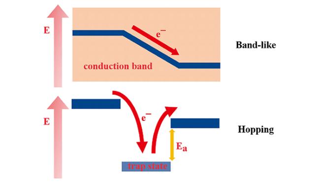
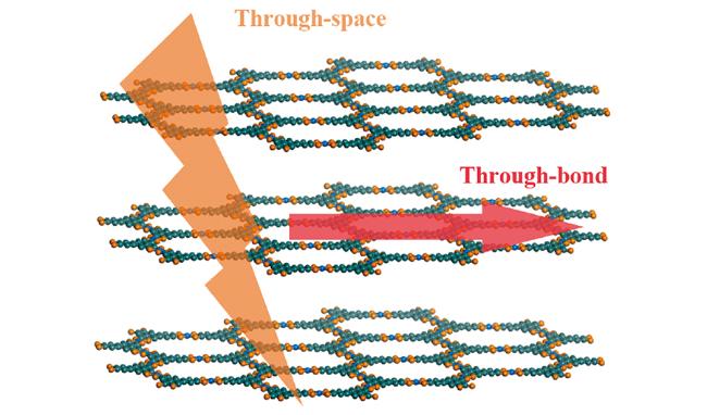
2.1 2D ECMOFs物理导电机制
2.2 2D ECMOFs化学导电机制
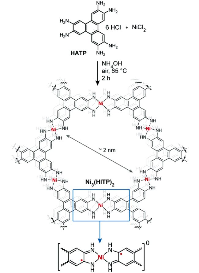
3 2D ECMOFs结构
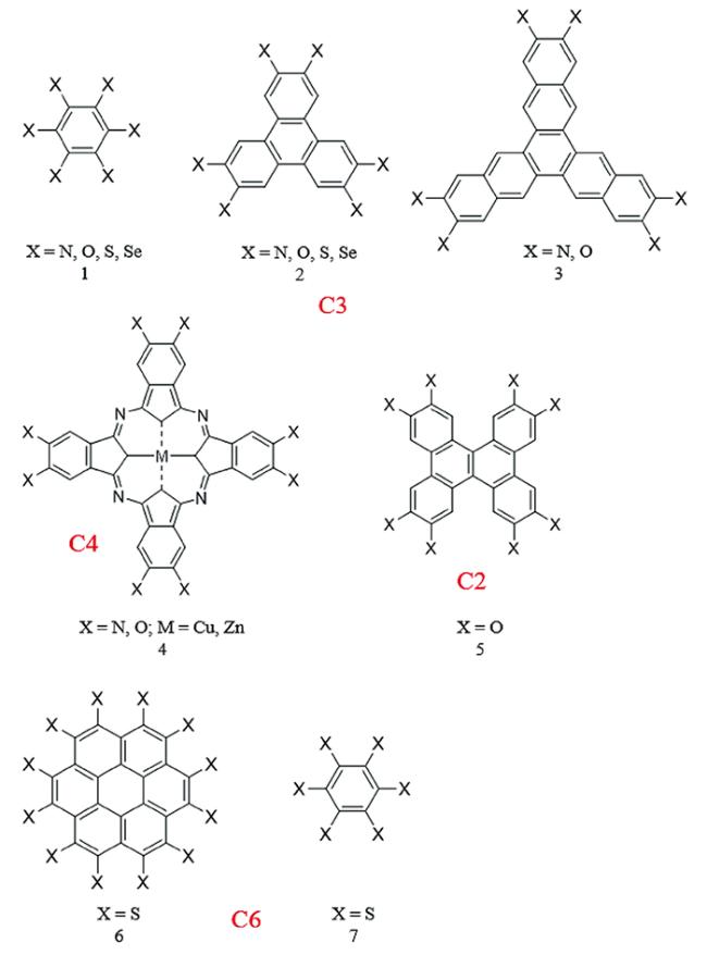
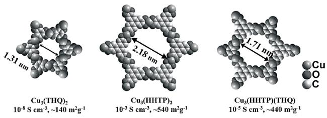
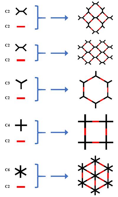
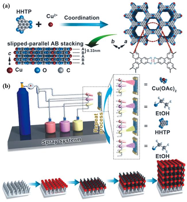
3.1 对称结构
3.2 不对称结构
3.2.1 双配体2D ECMOFs
3.2.2 合金2D ECMOFs
4 2D ECMOFs合成方法
4.1 单相合成方法
4.2 界面辅助合成方法
4.2.1 液/液界面
4.2.2 液/气界面
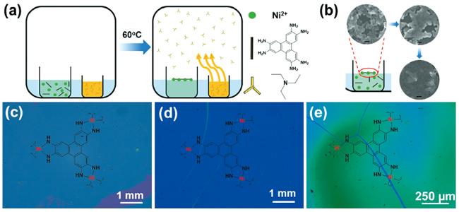
图7 (a)蒸气诱导合成Ni3(HITP)2薄膜示意图;(b)厘米级膜生长过程电子显微镜照片(标尺100 nm);(c~e)最薄膜、厚膜和最厚膜的光学照片[62]Fig. 7 (a) Schematic representation of the vapor-induced formation of Ni3(HITP)2 films;(b) SEM images of centimeter-scale film during the process of growth(scale bars: 100 nm); Optical images of(c) the thinnest film,(d) the thicker film, and(e) the thickest film[62]. Copyright 2019, WILEY-VCH Verlag GmbH & Co. KGaA, Weinheim |
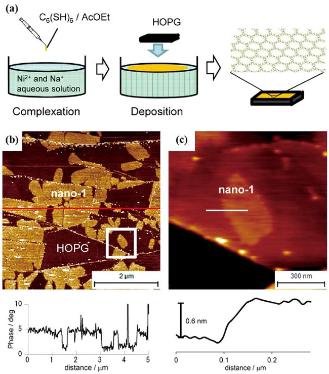
图8 单层Ni-BHT膜的合成与表征:(a)合成示意图;(b)在高取向热解石墨(HOPG)上的原子力显微镜(AFM)相位图及截面分析,亮区对应于Ni-BHT;(c)单层Ni-BHT的AFM结构图及截面分析,扫描范围为(b)中白色方框[17] Fig. 8 Synthesis and characterization of single-layer Ni-BHT. (a) Schematic illustration of the synthesis process;(b) AFM phase image on HOPG and its cross-sectional analysis. The bright areas correspond to Ni-BHT;(c) AFM topological image of single-layer Ni-BHT and its cross-sectional analysis. The white square in(b) corresponds to the scan area[17]. Copyright 2013, American Chemical Society |
4.2.3 固/液界面
4.2.4 其他界面
4.3 其他合成方法
5 2D ECMOFs应用
5.1 传感
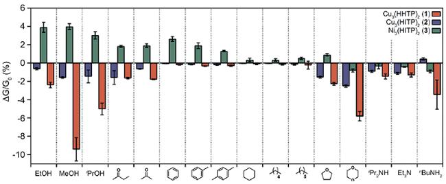
图10 基于Cu3(HHTP)2、Cu3(HITP)2和Ni3(HITP)2三种2D ECMOFs构建的气体传感阵列对不同种类代表性VOCs的传感性能对比,其中ΔG/G0是暴露在200 ppm VOCs气体中30 s的相对响应;每种响应为12次测试平均结果(针对每种ECMOF的3个独立器件进行4次测试),标准差由误差棒表示[33]Fig. 10 Sensing responses of the 2D ECMOF array based on Cu3(HHTP)2, Cu3(HITP)2 and Ni3(HITP)2 to representative examples from different categories of VOCs, where ΔG/G0 is the relative response(change in conductance) upon a 30 s exposure to 200 ppm of the VOC vapor; each response is averaged from 12 measurements(4 exposures to 3 separate devices for each ECMOF); error bars show one standard deviation[33]. Copyright 2015, American Chemical Society |
5.2 储能
5.2.1 超级电容器
5.2.2 电池
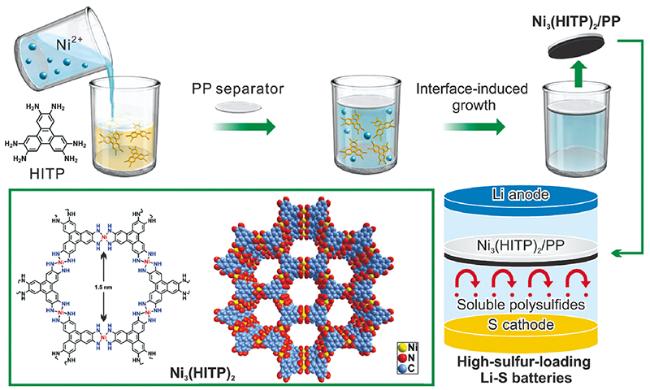
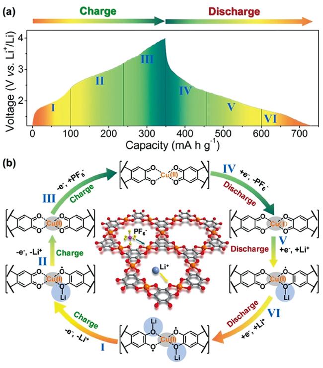
图12 (a)在50 mA·g-1下2D Cu-THQ MOF电极恒流充放电曲线,I-VI标记的六个区域对应(b)图中2D Cu-THQ MOF的各种充放电过程;(b)充放电过程中2D Cu-THQ MOF重复配位单元电子态的演变,蓝色和灰色圆圈分别表示Li和O之间的结合位点以及Cu的价态变化[88]Fig. 12 (a) Galvanostatic charge/discharge curves of 2D Cu-THQ MOF electrode at 50 mA·g-1. The six areas marked by I-VI represent the various charge/discharge processes of 2D Cu-THQ MOF marked in(b);(b) The evolution of electronic states of the repeating coordination unit of 2D Cu-THQ MOF during the charge/discharge process. The binding sites between Li and O, and variation of valence states of Cu, are indicated by blue and gray circles[88]. Copyright 2020, WILEY-VCH Verlag GmbH & Co. KGaA, Weinheim |
5.3 能源转换
5.4 电子器件
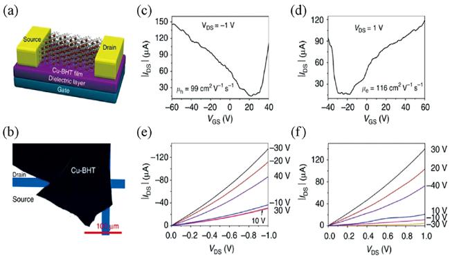
图13 (a)基于Cu-BHT的FET示意图;(b)底栅底接触FETs光学照片;(c,d)输出曲线;(e,f)转移曲线[5]Fig. 13 (a) Illustrative schematic of Cu-BHT-based field-effect transistors;(b) Photograph of bottom-gate bottom-contact FETs based on the Cu-BHT film;(c, d) Output and(e, f) transfer characteristics of Cu-BHT-based FETs[5]. Copyright 2015, Springer Nature |
图14 (a)基于2D ECMOF的垂直有机自旋阀器件(OSVs);(b)垂直OSV截面电子显微镜照片,包含50 nm LSMO、100 nm Cu3(HHTP)2、50 nm Co电极及50 nm Au;(c~e)10 K下LSMO/Cu3(HHTP)2(100 nm)/Co OSVs的磁滞回线、磁阻回线及磁阻温度依赖性曲线[106]Fig. 14 (a) Diagram of the 2D ECMOF-based vertical OSVs;(b) SEM image of the cross-section of the vertical OSV consisting of LSMO(50 nm), Cu3(HHTP)2 spacer(100 nm), Co electrode(50 nm), and Au(50 nm);(c) Magnetic hysteresis loops and(d) the magnetoresistance loop for the LSMO/Cu3(HHTP)2(100 nm)/Co OSVs at 10 K;(e) Temperature dependence of the magnetoresistance value[106]. Copyright 2020, WILEY-VCH Verlag GmbH & Co. KGaA, Weinheim |