


Contents
1 引言
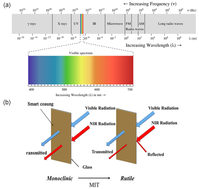
表1 常见的热致变色材料及其变色原理机理[16]Table 1 Common thermochromic materials and their discoloration principle mechanisms[16] |
| Thermochromic materials | Discoloration principle | Phase transition temperature |
|---|---|---|
| PNIPAm hydrogels | Critical temperature hydrophilic hydrophobic phase transition | 32 ℃ |
| IL-Ni-Cl Ionic liquid | Complex structure phase transition | Dark green(T>80 ℃) ↔ Light brown(T<20 ℃) |
| VO,VO2,VnO2n-1 (n=2~6,8) Ti2O3,TinO2n-1 (n=3~6) NbO2, Fe3O4, MnO2, CuO | xM++AOy+xe-↔ MxAOy (M=H, Li, Na; A=metal) | Yellow(T>68 ℃) ↔ Fuscous(T<6 ℃) Anatase ↔ Rutile(486~580 ℃) |
| Ag2S NiS | Still unknown | Monoclinic variant ↔ Equiaxed variant (179 ℃) cryogenic β phase ↔ α phase 397 ℃ |
| Ge-Te-Sb-S | Vitreous ↔ Crystal transfer | |
| Ge-S-Se, As-Se- (Ag,Cu) Cu2[HgI4] Ag2[HgI4] | Metal transfer in an uncertain structure structural change | Red(T>69 ℃) ↔ Dark purple(T<6 ℃) Yellow(T>48 ℃) ↔ Red(T< 5 ℃) |
2 热致变色材料
2.1 水凝胶
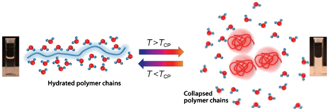
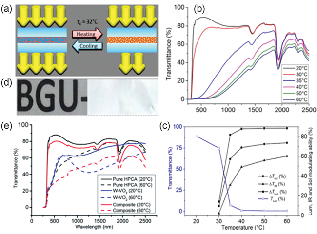
图3 (a) PNIPAm水凝胶智能窗夹层结构示意图;(b) 200 μm PNIPAm水凝胶薄膜不同温度的透射光谱;(c) 200 μm PNIPAm薄膜太阳光调控效率(ΔTsol),红外调控效率(ΔTIR)和可见光调控效率(ΔTlum);(d) 图左和右分别是20和80℃下200 μm薄膜的照片[42];(e) 25 μm HPCA, W-VO2, W-VO2-HPCA微凝胶样品透射光谱[37]Fig. 3 (a)Schematic diagram of the PNIPAm hydrogel smart window sandwich structure;(b)transmittance spectrum of 200 μm PNIPAm hydrogel thin film;(c)optical properties of integrated visible transmittance(Tlum), calculated solar energy modulation(ΔTsol), infrared modulation(ΔTIR), and integrated visible light modulation(ΔTlum) of 200 μm PNIPAm film;(d)the insets(left and right) are the 200 μm demonstration devices at 20 and 80℃, respectively[42];(a~d) reproduced with permission;(e)optical transmittance spectra of 25 μm HPCA, W-VO2, and W-VO2 with HPCA microgel samples[37] |
2.2 离子液体

图4 (a)纯IL-Ni-Cl膜、VO2纳米粒子膜和VO2/IL-Ni-Cl杂化膜在20℃和80℃透射光谱;(b)纯IL-Ni-Cl膜、VO2纳米粒子膜、VO2/IL-Ni-Cl杂化膜在20℃和80℃的照片[47];(c)透光率随温度变化示意图[52]Fig. 4 (a)Transmittance spectrum over the UV-Vis-NIR regions of pure IL-Ni-Cl film, VO2 nanoparticles, and VO2/IL-Ni-Cl hybrid film at 20 and 80 ℃;(b) demonstrations of pure IL-Ni-Cl film, VO2 nanoparticle film, and VO2/IL-Ni-Cl hybrid film at 20 and 80 ℃[47].(a、b) Reproduced with permission.(c)Schematic illustration of thermochromic optical transmittance change upon variation in temperature |
2.3 超材料

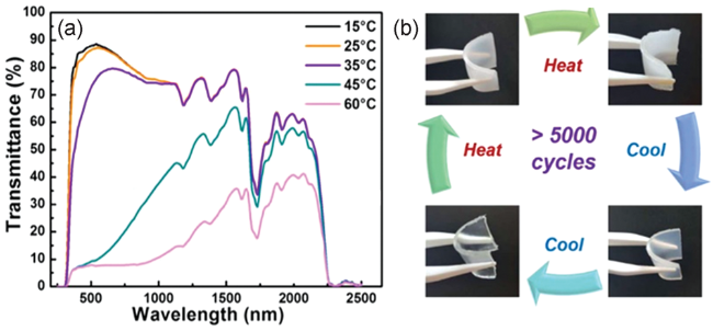
图6 (a)Kiri-kirigami结构示意图;(b)与a单轴拉伸时变形kiri-kirigami结构光学图像;(c)不同温度下kiri-kirigami超材料的热活化和定向开关实验演示[60]Fig. 6 (a)Schematic illustration of kiri-kirigami structure with notches on both sides. The upper part(green) has reversed patterned notches compared with the lower part(yellow).(b) Optical images of the deformed kiri-kirigami structure with identical design to(a) upon uniaxial stretching.(c) Experimental demonstrations of thermal activation and orientation switch of kiri-kirigami paper metamaterials at various temperatures[60] |
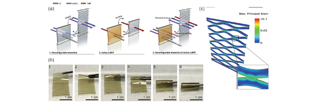
图7 (a)基于(1)可重构超材料、(2)有源LSPR和(3)有源LSPR与可重构超材料集成的透光率调节方法原理图;(b)复合膜卷起过程的照片(1~6);(c)SEM模拟kirigami VO2-PDMS薄膜的应变分布,插图为放大后的应变轮廓[61]Fig. 7 (a) Schematic of transmittance modulation methods based on(1) reconfigurable metamaterials,(2) active LSPR, and(3) the integration of active LSPR and reconfigurable metamaterials.(b)Photographs of the roll-up process of the yellow-brown composite film from figures on the left to right(1~6).(c)SEM-simulated strain distributions of the kirigami VO2-PDMS film and the magnified strain contour on a cut tip area as the inset[61] |
2.4 液晶
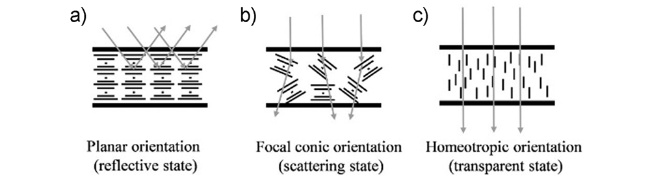
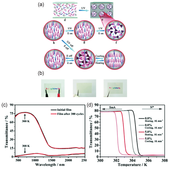
图9 (a)含有LCs和ITO NCs的晶胞中近晶相(SmA)向手性向列相(N*)转变的示意图;(b)薄膜随温度透明和不透明状态之间可逆改变;(c)初始膜(黑线)和300次循环后膜(红线)的透射光谱;(d)不含和含5.0 wt% ITO/SiO2的智能薄膜透光率随温度的变化关系[68]Fig. 9 (a)Schematic of the smectic A(SmA) to chiral nematic(N*) phase transition in a cell containing the LCs and ITO NCs;(b)the as-made film can reversibly change between transparent and opaque state in response to temperature;(c) the transmittance spectra of the initial film(black line) and the film after 300 cycles(red line);(d) temperature dependence of the transmittance of the smart films containing 0% ITO/SiO2 and 5.0 wt% ITO/Si |
2.5 二氧化钒(VO2)
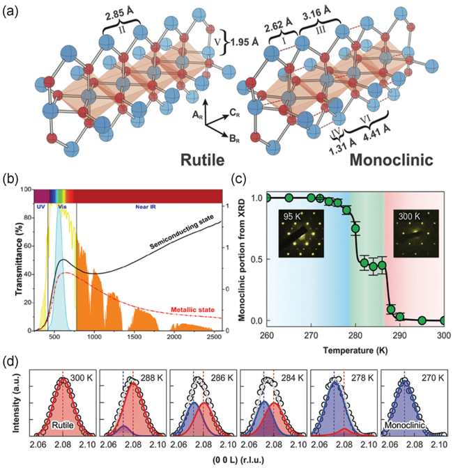
图10 (a)高温金属正方相R和低温绝缘单斜相M的原子结构示意图[74];(b)标准太阳能光谱[94];(c)几种温度下具有代表性的XRD峰;(d) 由图c的XRD衍射峰估算相对单斜部分温度的函数[75]Fig. 10 (a)The structure of rutile VO2(left) and monoclinic VO2(right)[73];(b)Standard solar spectra[92];(c) Representative XRD peaks at several temperatures.(d) Relative monoclinic portion as a function of temperature, estimated from XRD peak analysis in(c)[75] |

图11 不同温度下制备的样品SEM图像(a) 160℃,(b)180℃;不同钒前驱体浓度下产物的FE-SEM图像:(c) 0.17 M,(d) 0.25 M,(e) 1.0 M[93]Fig. 11 SEM images of samples prepared at different temperatures(a) 160℃ and(b) 180℃.Typical FE-SEM images of products obtained with different vanadium precursor concentrations.(c) 0.17 M,(d) 0.25 M,(e) 1.0 M[93] |
3 VO2智能涂层的表面工程构筑
3.1 有序阵列
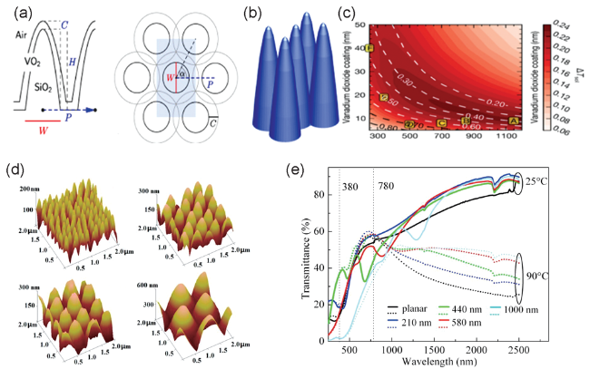
图12 (a) 六角形排列的圆形抛物面锥的纳米表面的侧面和正面图;(b)VO2涂层锥形阵列三维示意图;(c)基于FDTD参数计算得到的ΔTsol变化图[96];(d)不同周期的抗反射样品AFM图;(e)25 ℃和90 ℃测得的样品透射光谱[112]Fig. 12 (a)Side and top elevations of a nanotextured surface with hexagonally arranged circular paraboloid cones;(b) Three-dimensional illustration of the VO2-coated nipple arrays used in the simulation;(c) the calculated ΔTsol map based on the FDTD parameter search[96]. Reproduced with permission from Ref[96]Copyright The Optical Society;(d) AFM images of AR samples with different periods;(e) Transmittance spectra measured at 25/90 ℃ for planner and AR samples with 140 nm thickness[112] |
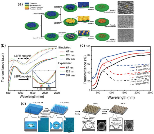
图13 (a)VO2纳米结构的制备工艺和由直径160 nm的PS球对应制备的VO2薄膜SEM图像;(b)67、125和287 nm的纳米颗粒阵列的计算和实测透射光谱[114];(c)在20和95 ℃下的透射光谱;(d)自模板制备高度有序蜂窝状结构过程[116]Fig. 13 (a) The preparation process of different periodical VO2 nanostructures; SEM images of patterned VO2 film prepared by the PS sphere with diameter of 160 nm;(b) Calculated(dashed lines) and measured(solid lines) transmittance spectra of nanoparticle arrays with diameters of 67, 125, and 287 nm, respectively;(c) the transmittance spectra at 20 and 95 ℃[114].(d) The preparation process of hollow-structured honeycomb-structured VO2 films via fully solution-based spontaneous self-template and assembly during the dual-phase transformation process[116] |
3.2 核@壳结构

图14 (a)VO2@TiO2复合工艺[120];(b) TLHNs结构的TEM图像[121];(c) VO2@ZnO核壳结构的TEM图像[122];(d) VO2@ZnS核壳纳米粒子结构示意图[123];(e,f)有/无良好色散的VO2及其相应的透射光谱[124];(g,h) VO2@SiO2纳米粒子和纳米棒的透射光谱[125]Fig. 14 (a) VO2@TiO2 composite[120];(b)TEM images of TLHNs structure[121].(c) TEM images of VO2@ZnO core-shell structure[122]. Reproduced with permission from Ref[120~122]. Copyright(2013) Nature,(2018)Wiley,(2017) ACS;(d) Schematic diagram of VO2 @ZnS core-shell nanoparticles[123];(e,f) VO2 with /without good dispersion and their corresponding transmittance spectra, respectively[124];(g,h)Transmittance spectra of VO2@SiO2 nanoparticles and nanorods, respectively[125].Reproduced with Permission from Ref[123~125]. Copyright(2017)Elsevier,(2015)ACS,(2013)Nanoscale |
3.3 复合技术
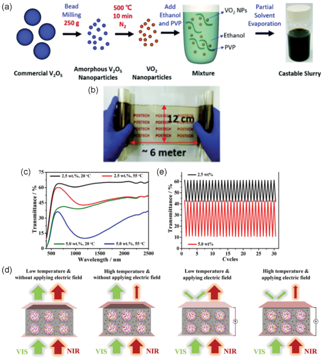
图15 (a)由 V2O5合成VO2纳米粒子;(b)大尺寸VO2-PVP涂层照片[129];(c)不同W-VO2纳米粒子含量的混合样品在20和55 ℃下透射光谱;(d)复合薄膜在不同刺激下的光调节方式;(e)不同W-VO2纳米粒子含量样品在冷热循环中的透过率[131]Fig. 15 (a) Preparation of VO2 nanoparticle-based mixture from commercial V2O5;(b) photograph of large-scale VO2-PVP coatings[129]. Copyright(2018) RSC.(c) optical transmittance spectra of hybrid samples with different W-VO2 NPs content at 20 ℃ and 55 ℃, respectively;(d) optical modulation modes of composite films in response to different stimuli;(e) transmittance of samples with different W-VO2 NPs content during heating and cooling cycles. Reproduced with permission from Ref[133]. Copyright(2017) ACS |
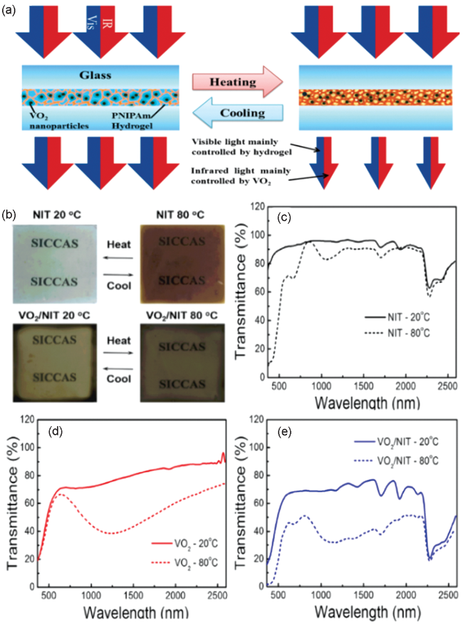
图16 (a) VO2/水凝胶混合膜的太阳光调节机制[35];(b) NIT和合成薄膜分别在20 ℃和80 ℃照片;(c) NIT涂层的透射光谱;(d) VO2单层膜透射光谱;(e) VO2/NIT复合膜透射光谱[135]Fig. 16 (a)Solar modulation mechanism of the VO2/hydrogel hybrid[35].(b)Photographs of NIT and composite films at 20 and 80 ℃, respectively. Transmittance spectra of(c) NIT coating;(d) VO2 single layer film;(e) VO2/NIT composite film. Reproduced with permission from Ref[135]. Copyright(2018) Elsevier |
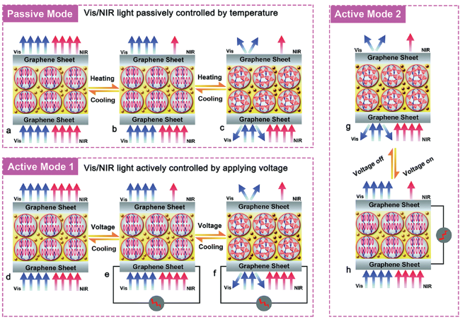
图17 (a~c)可见光透过率和近红外透过率分别以无源模式调制(对环境温度作出反应)的示意图;(d~f)在有源模式1下(对输入电压的响应),太阳光透过率从透明状态调制到阻挡状态的示意图;(g~h)响应外加电场将器件从不透明状态变为透明状态的示意图(工作在有源模式2)[136]Fig. 17 (a~c) Schematic illustration of the separated modulation of visible and NIR light transmittance working in passive mode(in response to environmental temperature);(d~f) Schematic illustration of the modulation of solar light transmittance from a transparent state to a blocking state working in active mode 1(in response to input voltage);(g and h) Schematic illustration of turning the device from an opaque state into a transparent state in response to the applied electric field(working in active mode 2)[136] |
表2 VO2涂层表面工程的研究成果总结Table 2 Summary of research results of VO2 coating surface engineering |
| Approach | Tlum(%) | ΔTsol(%) | Structure |
|---|---|---|---|
| Periodical patterned films | 43.6/59.9 | 19.4 | Moth-eye structure[111, 96] |
| 43.9/42.2 | 14.3 | Periodic micro-patterned VO2 thin films[137] | |
| 95.4#/- | 5.5 | Honeycomb-structured VO2(M) films[116] | |
| 46/45.8 | 13.2 | 2D periodical structure with d=160 nm[114] | |
| 70.2#/- | 7.9 | Ordered porous structure introduced by PS template[110] | |
| 75.5/73.8 | 7.7 | Double-sided island structure[138] | |
| 55.6 | 8.42 | VO2/SiO2 periodical structure[63] | |
| core-shell structure | 62.2/57.4 | 14.6 | SiO2@VO2 core-shell structure[124] |
| 62.6 | 18.54 | VO2@SiO2 nano-rods[127] | |
| 71.02/56.5 | 14.31 | VO2@SiO2 core-shell structure[139] | |
| 51/- | 19 | VO2@ZnO core-shell structure[122] | |
| - | - | VO2@ZnS core-shell structure[123] | |
| 74 | 12 | SiO2/TiO2/VO2 hollow core-shell nanospheres structure | |
| 61.8 | 12.6 | VO2@SiO2 hollow core-shell sphere structure[127] | |
| Integrated techniques | - | 12.9 | VO2 dispersed in PVP[129] |
| 43/- | 11.3 | SiO2-VO2 composite film[140] | |
| 57.8/- 73.3/68.71 | 34.6 18.19 | Embedding VO2 NPs into LCs matrix[131] | |
| 67.3/36.2 | 27.3 | Hybrid of VO2 and nickel(II)-based ligand[135] VO2/hydrogel hybrid film[35] | |
| 62.6/43.2 | 34.7 | ||
| 80/33 | 36 | VO2 /microgels hybrid[37] | |
| 55.3 | 40.9 | PC-LCs/VO2/graphene composite structure[137] | |
| 35.2 | 37.7 | Kirigami Metamaterials[61] |