


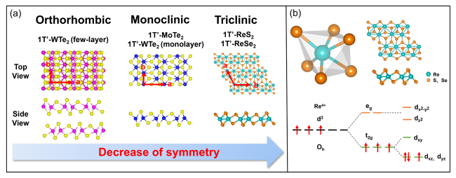
1 引言
2 1T'-MTe2(M=Mo、W)
2.1 1T'-MTe2的CVD制备
2.1.1 金属单质前驱体
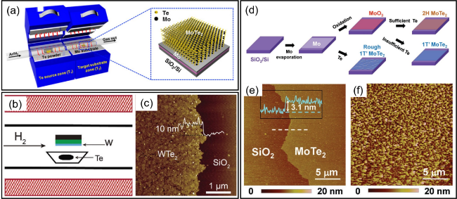
图2 (a) 用Mo膜合成1T'-MoTe2薄膜的实验装置示意图,插图是在SiO2/Si衬底上的1T'-MoTe2薄膜的示意图[34]; (b) 用W膜合成1T'-WTe2薄膜的实验装置示意图[35]; (c) 用2 nm的W种子层生长的1T'-WTe2的AFM图像[35]; (d) 以Mo和MoO3为前驱体制备1T'-MoTe2的过程示意图[45]; (e,f) 以Mo和MoO3为前驱体生长的1T'-MoTe2的AFM图像[45]Fig. 2 (a) Schematic diagram of the experimental setup for the synthesis of the 1T'-MoTe2 film by Mo film. Inset is a schematic diagram of the 1T'-MoTe2 film on a SiO2/Si substrate[34], Copyright 2015, American Chemistry Society; (b) Schematic diagram of the experimental setup for the synthesis of the 1T'-WTe2 film by W film[35]; (c) AFM images of as-grown 1T'-WTe2 from a 2 nm W seed layer[35], Copyright 2017, John Wiley & Sons, Inc; (d) Schematic diagram of the growth process for 1T'-MoTe2 using Mo and MoO3 as precursors[45]; (e, f) AFM image of the 1T'-MoTe2 film grown from MoO3 and Mo, respectively[45], Copyright 2016, John Wiley & Sons, Inc |
2.1.2 金属氧化物前驱体
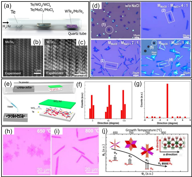
图3 (a) 低熔点共晶法辅助生长1T'-MoTe2和1T'-WTe2原子层的实验装置示意图[29]; (b, c) 少层1T'-MoTe2和1T'-WTe2的STEM实验图像[29]; (d) 不同比值的MoO3和NaCl混合物反应产物的光学显微镜图像[38]; (e) 水辅助法生长1T'-WTe2原子层的实验装置示意图[42]; (f, g) 1T'-WTe2在c面和a面蓝宝石衬底上的生长取向统计分布直方图[42]; (h, i) 650和800 ℃合成的1T'-MoTe2的光学显微图像[40]; (j) 生长温度升高过程中形貌变化和沿两个方向生长速率(υa和υb)变化的示意图,插图为1T'-MoTe2纳米带的球棒模型[40]Fig. 3 (a) Schematic diagram of experimental setup for the assisted growth of the 1T'-MoTe2 and 1T'-WTe2 atomic layers by low melting point eutectic method[29]. (b, c) Experimental STEM image of 1T'-MoTe2 and 1T'-WTe2 few layer[29], Copyright 2017, John Wiley & Sons, Inc. (d) Optical microscope images of the reaction products with different molar ratios of MoO3 and NaCl mixtures[38], Copyright 2017, Springer Nature. (e) Schematic diagram of experimental setup for the growth of the 1T'-WTe2 atomic layers by water-assisted methods[42]. (f, g) Histogram of growth orientation statistical distribution of 1T'-WTe2 on the c-plane and a-plane sapphire substrate[42], Copyright 2022, IOP Publishing. (h, i) Optical microscopic images of 1T'-MoTe2 synthesized at 650 and 800 ℃[40]. (j) Schematic diagram of morphology and growth rate in two direction evolution (υa and υb) during the growth temperature increasing[40] (the inset is the ball-and-stick model of 1T'-MoTe2 nanoribbon), Copyright 2020, RSC Publishing |
2.1.3 金属铵盐前驱体
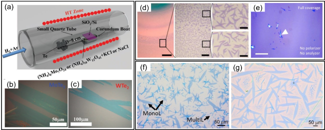
图4 (a) 用铵盐粉末合成1T'-MoTe2和1T'-WTe2原子层的实验装置示意图[53]; (b, c) 大面积1T'-MoTe2(长≈200 µm,宽≈50 µm)和1T'-WTe2 (长≈320 µm,宽≈80 µm)晶体的光学显微镜图像[53]; (d) 通过液滴法生长的1T'-MoTe2薄片的光学显微图像,比例尺分别为200、40和10 μm[56]; (e) 完全覆盖的1T'-MoTe2的光学显微图像,白色箭头表示薄片的一小块多层区域[59]; (f, g) 氧等离子体处理前后SiO2/Si基底上生长的1T'-MoTe2的光学显微图像[60]Fig. 4 (a) Schematic diagram of the experimental setup for the synthesis of the 1T'-MoTe2 and 1T'-WTe2 atomic layers by ammonium salt powder[53]. (b, c) Optical microscope images of large-area 1T'-MoTe2 (length ≈ 200 µm and width ≈ 50 µm) and 1T'-WTe2 (length ≈ 320 µm and width ≈ 80 µm) crystals[53], Copyright 2017, John Wiley & Sons, Inc. (d) Optical micrograph images of 1T'-MoTe2 flakes grown by the droplet method. Scale bars are 200, 40, and 10 μm, respectively[56], Copyright 2016, American Chemistry Society. (e) Optical micrograph image of fully covered 1T'-MoTe2, white arrow indicates a small portion of multilayer flakes[59], Copyright 2016, IOP Publishing. (f, g) Optical microscopic image of 1T'-MoTe2 grown on SiO2/Si substrate before and after oxygen plasma treatment[60], Copyright 2021, American Chemistry Society |
2.2 MTe2的相调控
2.2.1 应变调控
2.2.2 温度调控
3 1T'-ReX2 (X=S, Se)
3.1 铼前驱体

图6 (a) 生长时间为10 min时二维1T'-ReS2产物的典型OM图像[73]; (b) 1T'-ReS2薄膜的光学显微镜图像[74]; (c) CVD制备二维1T'-ReS2的装置示意图[75]; (d) Te辅助CVD生长方法的装置示意图[76]; (e) 转移至SiO2/Si基底表面的单层1T'-ReS2光镜图像[76]; (f) 厚度为1 nm的单层1T'-ReS2的光学显微图像[77]; (g,h) 在SiO2/Si基底表面生长的1T'-ReS2、1T'-ReSe2的光学图像; (i) 对应图(h)中虚线框的放大图[78]; (j) VRe-1T'-ReS2的STEM图像,插图为对应的FFT图像[79]Fig. 6 (a) Typical OM images of 2D 1T'-ReS2 at a growth period of 10 min[73], Copyright 2015, John Wiley & Sons, Inc. (b) Optical microscopy images of 1T'-ReS2 films[74], Copyright 2020, IOP Publishing. (c) Schematic of growth approach of 2D 1T'-ReS2 by CVD[75], Copyright 2017, RSC Publishing. (d) Schematic of apparatus for the growth of 2D 1T'-ReS2 by Te-assisted CVD[76]. (e) Optical images of monolayer 1T'-ReS2 transferred to SiO2/Si[76], Copyright 2016, John Wiley & Sons, Inc. (f) Optical microscopic image of monolayer 1T'-ReS2 with thickness of 1 nm[77], Copyright 2019, AIP Publishing. (g, h) Optical images of 1T'-ReS2 and 1T'-ReSe2 grown on the surface of SiO2/Si substrate. (i) Enlargement of the dashed box in figure (h)[78], Copyright 2020, RSC Publishing. (j) STEM image of VRe-1T'-ReS2 with inset corresponding FFT image[79], Copyright 2018, American Chemistry Society |
3.2 三氧化铼前驱体
3.2.1 绝缘基底

图7 (a) 蓝宝石基底表面生长双层1T'-ReS2薄膜的光学显微图像[80]; (b) SiO2/Si基底表面生长的1T'-ReSe2薄片的光学显微图像[81]; (c) 空间限域法在云母基底表面制备1T'-ReS2的装置示意图[85]; (d) 生长在SiO2/Si基底表面的向日葵形状1T'-ReSe2的光学显微图像[87]; (e) 生长在SiO2/Si基底表面的截断三角形状1T'-ReSe2 的光学显微图像[87]; (f) 通过钠盐辅助CVD法在蓝宝石基底表面合成单层1T'-ReSe2产物[88]; (g) 多晶晶界处的高分辨ADF-STEM图像[25]; (h) 两个平行晶粒间沿b轴方向延伸形成重叠晶界ADF-STEM图像[90]; (i) 裂纹行进的ADF-STEM图像[91]Fig. 7 (a) Optical micrographs of bilayer 1T'-ReS2 films grown on sapphire[80], Copyright 2016, John Wiley & Sons, Inc. (b) OM image of 1T'-ReSe2 flakes grown on SiO2/Si[81], Copyright 2016, John Wiley & Sons, Inc. (c) Schematic diagram of the device for the Growth of 1T'-ReS2 on mica by the space-limited method[85], Copyright 2016, RSC Publishing. (d) Sunflower-shaped 1T'-ReSe2 grown on SiO2/Si substrates[87]. (e) Optical microscopy of truncated triangular-shaped 1T'-ReSe2 grown on SiO2/Si[87], Copyright 2018, Springer Nature. (f) Synthesis of monolayer 1T'-ReSe2 products on the surface of sapphire by sodium salt-assisted CVD[88], Copyright 2020, Springer Nature. (g) High-resolution ADF- STEM images at polycrystalline grain boundaries[25], Copyright 2019, John Wiley & Sons, Inc. (h) ADF-STEM images of overlapping GB formed by two parallel grains extending along the b-axis[90], Copyright 2020, Elsevier; (i) ADF-STEM images of crack marching[91], Copyright 2021, John Wiley & Sons, Inc |
3.2.2 金属基底

图8 (a) 在Au箔基底的表面生长1T'-ReSe2的示意图[92]; (b) 金箔基底表面生长平1T'-ReSe2薄片的SEM图像[95]; (c) Vsample 值为20 mV时单晶1T'-ReSe2的STM图像[95]; (d) 两个相邻1T'-ReSe2晶畴之间的平行位错组成的晶界图像[96]; (e) 孪晶界的STM图像[96]; (f~h) 在Au(111)、Au(001)及Au(101)晶面表面生长的单层1T'-ReS2的SEM图像[97]; (i) 在柔性玻璃表面生长的从2层到8层的1T'-ReS2薄膜图像[98]Fig. 8 (a) Schematic diagram of growth of 1T'-ReSe2 on Au foil substrates[92], Copyright 2018, IOP Publishing. (b) SEM image of 1T'-ReSe2 sheet on a gold foil substrate[95]. (c) STM image of single-crystal 1T'-ReSe2 at a Vsample value of 20 mV[95], Copyright 2018, American Chemistry Society. (d) Two adjacent ReSe2 domains between GB images consisting of parallel dislocations[96]. (e) STM images of twinned GB[96], Copyright 2018, Springer Nature. (f-h) SEM images of 1T'-ReS2 grown on Au(111), Au(001) and Au(101) crystalline surfaces[97], Copyright 2021, John Wiley & Sons, Inc. (i) Optical images of 1T'-ReS2 films grown on a flexible glass surface from 2 to 8 layers[98], Copyright 2017, IOP Publishing |
3.2.3 其他种类基底
3.3 高铼酸铵前驱体

图9 (a, b) 二维1T'-ReS2的SEM图像及原子序数衬度像[100]; (c,d) (截断)三角形及六边形1T'-ReS2晶畴的光学显微图像[101]; (e) 单层1T'-ReSe2的光学显微图像,比例尺为10 μm; (f) 对应图(e)中1T'-ReSe2的TEM高角环形暗场( HAADF )图像,比例尺为10 μm[102]; (g) 转移至SiO2/Si基底表面单层1T'-ReS2晶粒的OM图像,比例尺为5 μm[103]; (h) 六边形单层1T'-ReS2晶畴的光学图像;(i)六边形晶畴动力学生长过程示意图[104]; (j) 1T'-ReS2片的生长过程示意图[105]Fig. 9 (a, b) SEM images and Z-contrast STEM images of two-dimensional 1T'-ReS2[100], Copyright 2015, John Wiley & Sons, Inc. (c, d) Optical microscopy images of (truncated) triangular and hexagonal 1T'-ReS2 crystal domains[101], Copyright 2016, American Chemistry Society. (e) Optical microscopy images of monolayer 1T'-ReSe2, scale bar is 10 μm. (f) High-angle annular dark field ( HAADF) TEM image of 1T'-ReSe2 corresponding to Figure (e), scale bar is 10 μm[102], Copyright 2021, American Chemistry Society. (g) OM image of a monolayer of 1T'-ReS2 grains transferred to SiO2/Si at a scale of 5 μm[103], Copyright 2020, American Association for the Advancement of Science. (h) Optical image of a hexagonal monolayer of 1T'-ReS2 crystal domains. (i) Schematic kinetic growth process of hexagonal crystal domains[104], Copyright 2020, American Chemistry Society. (j) Schematic of the growth process of 1T'-ReS2 sheets[105], Copyright 2018, John Wiley & Sons, Inc |