


1 引言
2 弹性体介电层材料的类型
3 微结构化弹性体介电层的制备
3.1 多孔弹性体介电层的制备方法
3.1.1 固体模板法
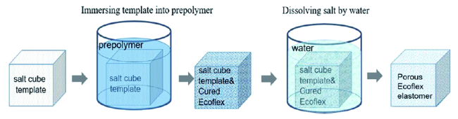
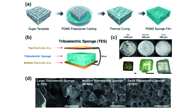
图2 (a) 使用糖模板制作摩擦电海绵(Triboelectric Sponge, TES)的示意图。(b) 由TES制作的纳米发电机的模型图。(c) 使用不同类型的糖颗粒作为PDMS海绵的模板。标尺为200 μm。(d) 三种TES的扫描电子显微镜(SEM)图,标尺为500 μm [53]Fig.2 (a) Schematic illustration of the fabrication procedure of the porous PDMS sponge using sugar particles. (b) Conceptual model of the triboelectric sponge(TES) with an embedded generator. (c) Various types of sugar particles were used as templates for the PDMS sponge films. All of the scale bars(black) shown in the figures are 200 μm. (d) Morphologies of three types of TESs using scanning electron microscope. All of the scale bars(white) shown in the figures are 500 μm [53].(Copyright 2016, Wiley Online Library) |
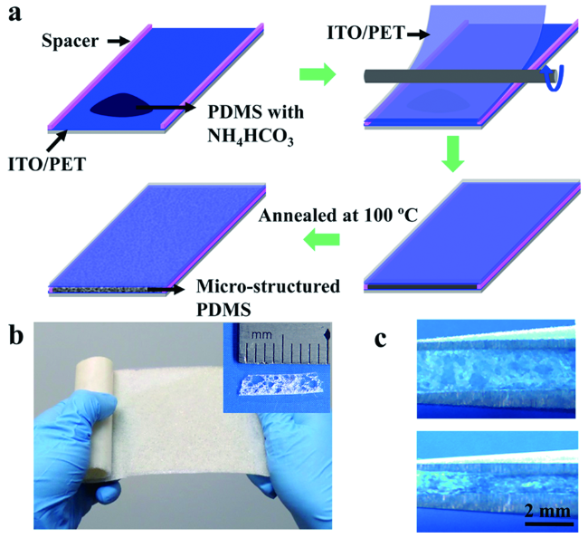
图3 微结构PDMS薄膜的制备及电容式压力传感器的制作过程。(a)一步法制备微结构PDMS薄膜的示意图。(b)大面积微结构PDMS薄膜的照片(内插图为微结构PDMS胶片的横截面照片)。(c) 使用镊子夹持微结构PDMS薄膜,不施加(上图)和施加(下图)压力作用下薄膜的横截面照片[56]Fig.3 Fabrication of the micro-structured PDMS film and the capacitive pressure sensors.(a) Schematic illustration of one-step processing of the micro-structured PDMS film based on a mixture of PDMS prepolymer and its curing agent with ammonium bicarbonate(NH4HCO3) and its seamless integration into the process flow for fabricating a flexible capacitive sensor.(b) The photo image of the fabricated large area micro-structured PDMS film(the inset shows the cross-sectional photo image of the micro-structured PDMS film).(c) The cross-sectional photo images of the micro-structured PDMS film clipped by a tweezer without pressure(upper) and with pressure(bottom)[56].(Copyright 2016, American Chemical Society) |
3.1.2 其他模板法
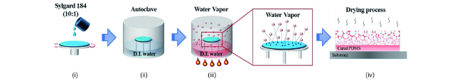
图5 VEC法制备PDMS双介电层的示意图。(i) PDMS预聚体和固化剂的旋涂,(ii) 在高压釜中用去离子水密封样品,(iii) 通过加热高压釜产生水蒸气。放大图显示:水蒸气渗透到未固化的PDMS薄膜中,(iv) 双介电层的固化过程图[63]Fig.5 Fabrication process of the double dielectric layer composed of the porous and dense PDMS films via vapor encapsulation casting. (i) Spin-coating of uncured PDMS solution.(ii) Sealing the sample with D.I. water in the autoclave.(iii) Heating the autoclave to produce water vapor. Magnified image shows that water vapor penetrates into the uncured PDMS film.(iv) Curing of the double dielectric layer[63].(Copyright 2019, Elsevier) |
3.2 非多孔阵列型弹性体介电层的制备方法
3.2.1 硅模板法
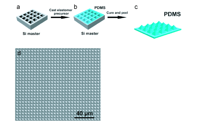
图6 触觉传感器的制作原理图。(a) 采用传统的光刻方法在硅片上制备了凹槽金字塔阵列结构。(b) PDMS预聚体浇注在硅模板上。(c) PDMS膜固化后从硅模板上剥离。(d) 具有金字塔图案阵列的PDMS薄膜的SEM图[66]Fig.6 Schematic illustration of the tactile sensor device fabrication. (a) Si masters with recessed pyramid microstructures are fabricated by conventional lithography methods. (b) PDMS precursor is cast on the Si masters. (c) Freestanding PDMS films with microstructures are cured and peeled off from Si masters. (d) SEM image of PDMS with uniform pyramid pattern arrays[66]. (Copyright 2014, Wiley Online Library) |
3.2.2 其他模板法
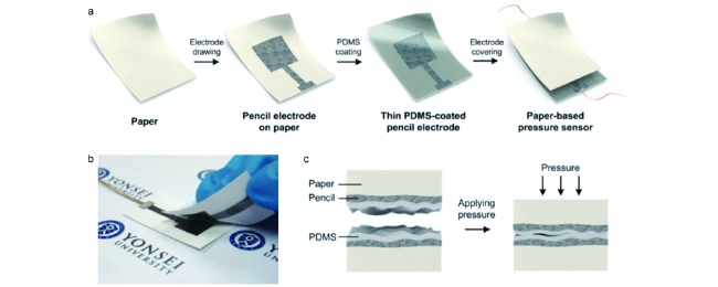
图7 (a) 纸基电容式压力传感器的制作流程图。(b) 压力传感器的制作照片。(c) 施加压力时压力传感器的示意图[72]Fig.7 (a) Schematic process for the fabrication of the paper-based capacitive pressure sensor. (b) Photograph of the fabricated pressure sensor. (c) Schematic depiction of the pressure sensor under applied pressure[72]. (Copyright 2010, Wiley Online Library) |
表1 各类模板法的优缺点及代表性微结构化弹性体形貌Table 1 Advantages and disadvantages of different template methods and representative morphologies of the micro-structured elastomers |
| Template method | Advantages | Disadvantages | Morphology of the structured elastomer | Representative work |
|---|---|---|---|---|
| Sugar template method | Simple preparation and low cost | If the sugar is not completely dissolved, it would introduce an undesirable viscosity in the dielectric layer | 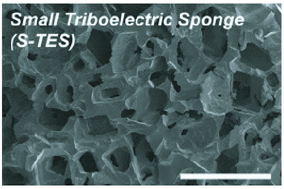 | Yang-Kyu Choi, et al[52]. |
| Sodium chloride template method | Easy dispersion of templates within the elastomer | Poor manipulation on the pore morphology | 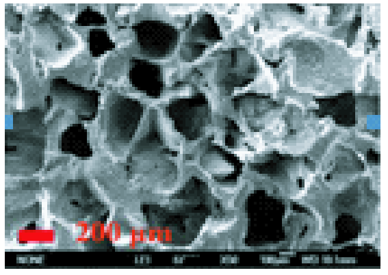 | Yongtao Tian, et al[47]. |
| Bicarbonate template method | Resulting product can be dissolved by water, no residue | The preparation process releases NH4 and CO2, not environment-friendly | 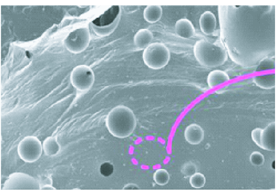 | Qiulin Tan, et al[57]. |
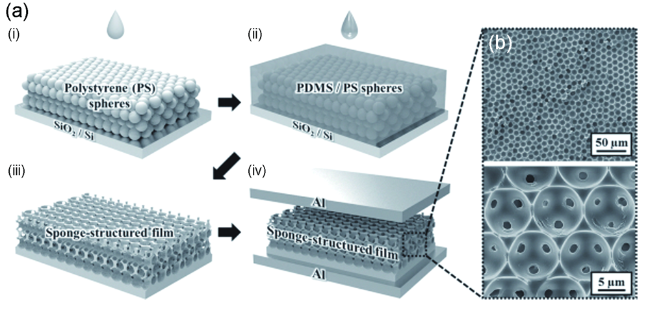
| Microsphere template method | Uniform pores | Templates are not easy to remove after the complete of templating | 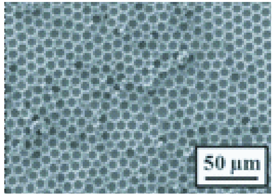 | Jeong Min Baik, et al[59]. |
| Silicon template method | Uniform structures, and the mould can be used repeatedly | Complex and expensive manufacturing process, not conducive to mass production | 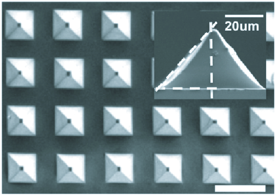 | Zhenan Bao, et al[24]. |
4 微结构化弹性体介电层的应用
4.1 微结构化弹性体介电层的传感应用
4.1.1 多孔弹性体介电层的传感应用
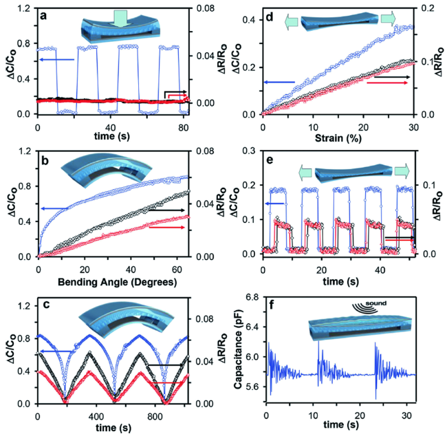
图8 PDMS/CNT复合压力传感器对于多种机械刺激的检测。(a) 在2 kPa压力的周期性作用下,电容和电阻随时间的变化曲线。(b) 电容和电阻随不同弯曲角度(0 ~ 65°)的变化曲线。(c) 弯曲角度在0 ~ 65°时,电容和电阻随时间的变化。(d) 电容和电阻随横向应变的变化曲线。(e) 在重复应变为15% 时,电容和电阻随时间的变化曲线。(f) 在敲击吉他弦的声音振动下,电容和电阻随时间的变化曲线。(a~e) 电容变化、上电极电阻变化和下电极电阻变化分别用蓝色圆圈、黑色方块和红色三角形表示[13]Fig.8 Detection of various mechanical stimuli. (a) Capacitance and film resistances as a function of time under repeated normal pressure of 2 kPa. (b) Capacitance and film resistances as a function of bending angle from 0 to 65°. (c) Capacitance and film resistances as a function of time at incrementally increasing and decreasing bending angle from 0 to 65°. (d) Capacitance and film resistances as a function of percent strained laterally and (e) as a function of time at repeated strain of 15%. (f) Capacitance as a function of time under sound vibration due to hitting a guitar string. (a~e) Change in capacitance, change in top electrode resistance, and change in bottom electrode resistance are represented as blue circles, black diamonds, and red triangles, respectively[13].(Copyright 2014, Wiley Online Library) |
4.1.2 非多孔阵列型弹性体介电层的传感应用
4.2 微结构化弹性体介电层的纳米发电机应用
4.2.1 多孔弹性体介电层的纳米发电机应用
4.2.2 非多孔阵列型弹性体介电层的纳米发电机应用
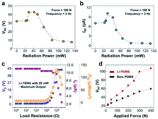
图9 LI-TENGs的电输出特性:(a)开路电压。(b)LI-TENGs在0 ~ 132 mW激光功率范围内的短路电流。(c)负载电阻(RL)与LI-TENG(29 mW)输出电压和电流的相关性。(d)TENG和LI-TENG(29 mW)的开路电压随外界压力的变化[83]Fig.9 Electrical output characteristics of the fabricated LI-TENGs:(a) open-circuit voltage,(b) short-circuit current of the fabricated LI-TENGs with laser power levels ranging from 0 to 132 mW.(c) RL dependency of the output voltage and current of the LI-TENG(29 mW).(d) Open-circuit voltage of the bare TENG and the LI-TENG(29 mW) according to the external force[83].(Copyright 2017, Elsevier) |